

Single and multi-junction light and carrier collection management cells
a technology of carrier collection and light, applied in the field of photovoltaic devices for energy conversion, can solve the problems of high cost and complexity, high cost of power conversion efficiencies, and ineffective capture of light in cells, and achieve the effect of enhancing the trapping of impinging ligh
- Summary
- Abstract
- Description
- Claims
- Application Information
AI Technical Summary
Benefits of technology
Problems solved by technology
Method used
Image

Examples
example 1
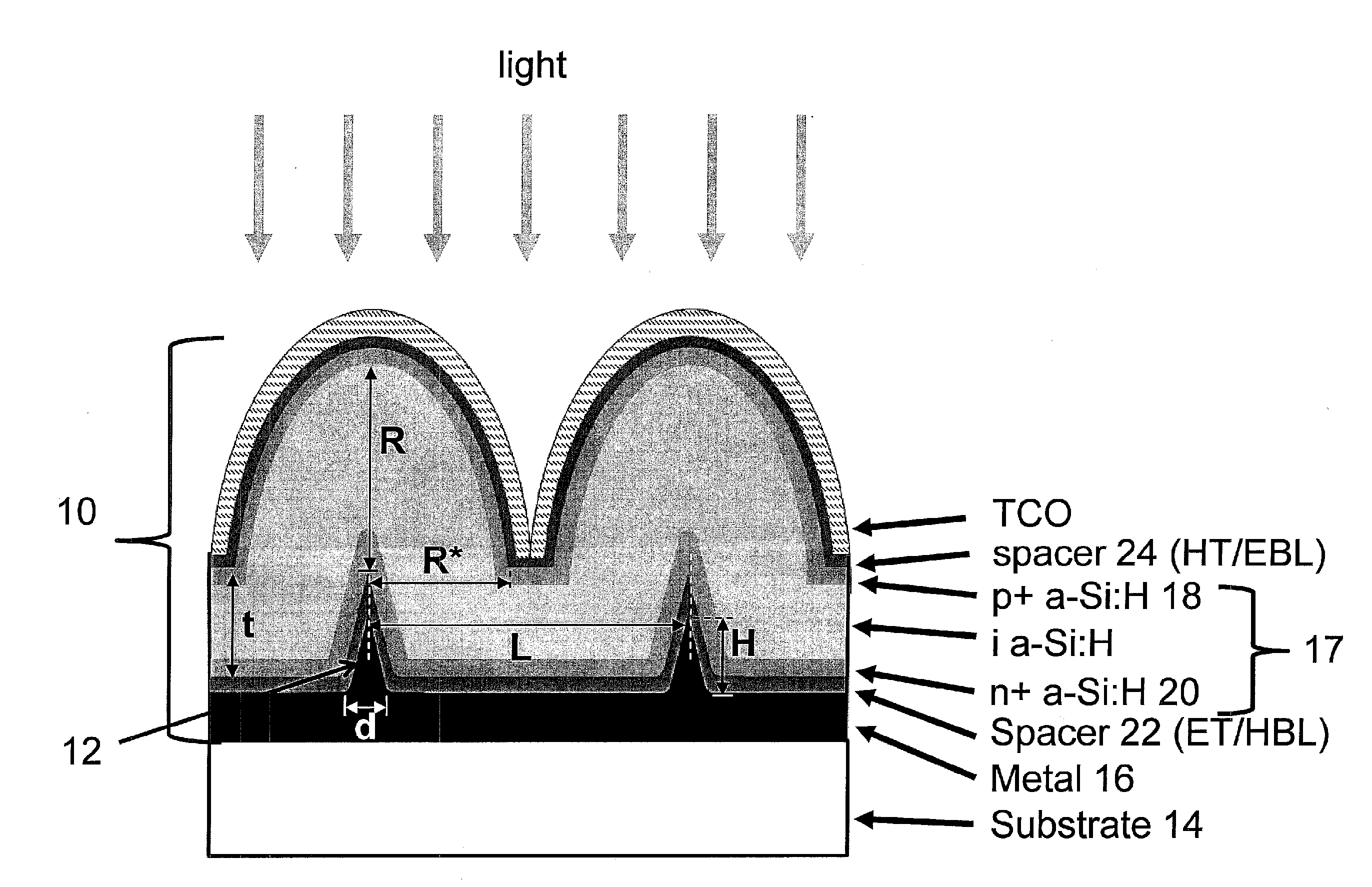
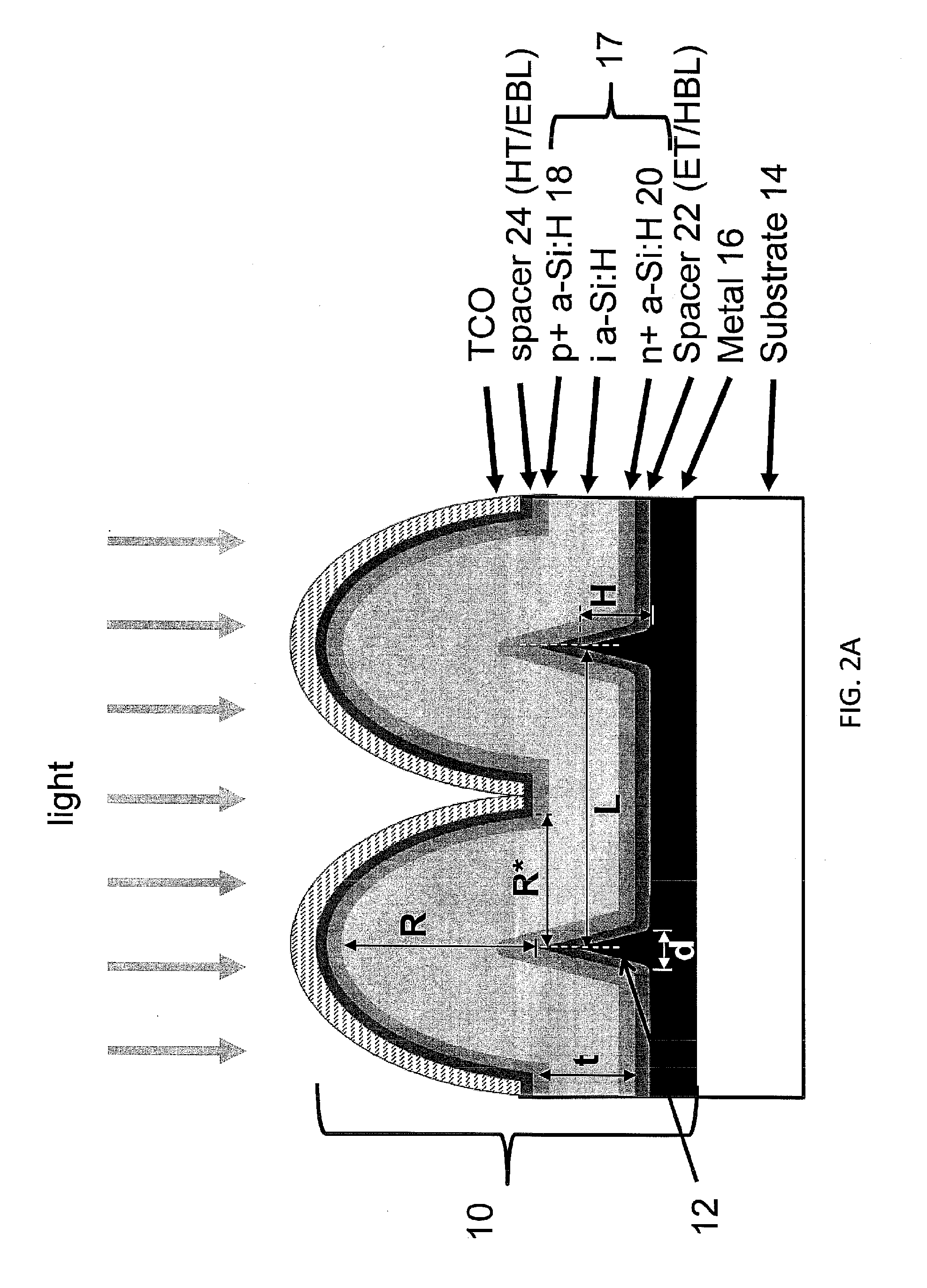
[0033]Plasma enhanced chemical vapor deposited (PECVD) a-Si:H was used as the absorber in superstrate single junction structures. Atomic layer deposition (ALD) was first used to coat the indium tin oxide (ITO) on a glass substrate with transparent, conducting aluminum zinc oxide (AZO). This AZO served as an optical spacing layer, as hole transport layer, and as protection for the hydrogen plasma-sensitive ITO during a-Si:H PECVD from silane type gases. These materials are appreciated to be exemplary and that alternative materials with similar optical and electrical properties are readily substituted by a routineer in the art. After applying a template material, void regions were created in the template by standard e-beam lithography-based processing and ALD was used to produce AZO nano-elements in each template void region, thereby resulting in an array of AZO conducting, but transparent nano-elements protruding from the ITO electrode. The array of such nano-elements can be discerne...
example 2
[0035]Computer modeling work on both single junction and multi-junction LCCM solar cell structures (a-Si:H, nc-Si:H, and tandem a-Si:H / a-Si(1-x) / Ge(x):H) shows the benefits resulting from the incorporation of nanostructures according to the architecture of this invention (i.e., LCCM approach versus planar controls). In all cases, the LCCM approach outperforms the planar controls. FIG. 5 gives the absorption as a function of wavelength for a single-junction nano-crystalline silicon (nc-Si) superstrate LCCM structure and for the corresponding nc-Si planar structure. These plots are computer modeling results obtained for an inventive design simulated with Maxwell's equations solver software and expertise available at the University of Arkansas (UA). These results are for single junction cells and they drive home an important point: the LCCM architecture greatly enhances absorption, particularly at long wavelengths—and it is doing so in FIG. 5 for a 400 nm nc-Si deposition.
example 3
[0036]FIG. 6 gives an LCCM substrate Configuration 1 single junction cell which, by definition, has the light entry through the top (80 nm AZO) anode. The cell has 100 nm diameter aluminum zinc oxide (AZO) columns as the nano-elements which are sitting on a cathode composed of 5 or 30 nm of AZO coated onto an opaque planar Ag film. The transport function of this AZO coating is to serve as an electron transport / hole blocking layer (ET / HBL) at the cathode. It also has an optical function, as will emerge in our discussion of the JSC response versus nano-element spacing L obtained from modeling. This response is given in FIG. 6 for the two ET / HBL thicknesses. As seen, JSC decreases with decreasing L for Ltouch and has two maxima in the range L≧Ltouch one of which is an absolute maximum near L˜Ltouch. The quantity Ltouch is the specific L for which the domes just touch. The JSC dependence on L in the L>Ltouch range present in FIG. 6 is very different from that of superstrate structures w...
PUM
 Abstract
Description
Claims
Application Information