Plasma processing device

a processing device and plasma technology, applied in the field of plasma processing devices, can solve the problems of reducing the density of the film, forming more defects in the film, and difficult to generate high-density atomic hydrogen radicals, so as to achieve easy control of the energy distribution of electrons and reduce the density of electrons.

Inactive Publication Date: 2013-08-01
ELECTRO-MOTIVE DIESEL
View PDF14 Cites 8 Cited by
  • Summary
  • Abstract
  • Description
  • Claims
  • Application Information

AI Technical Summary

Benefits of technology

[0015]The plasma processing device according to the present invention is characterized in that the energy distribution of the electrons in the plasma can be controlled by regulating the distance between the plasma control plate provided in the plasma producing chamber and the radio-frequency antenna installed in the same chamber. When the plasma control plate is moved closer to the radio-frequency antenna, a portion of the electrons in the plasma produced in the plasma producing chamber disappear due to their collision with the plasma control plate, so that the electron density decreases. This decrease in the e

Problems solved by technology

The production of such radicals having high sticking coefficients leads to the formation of defects in the film or a decrease in the film density.
It also causes the problem that high-order silane radicals (SixHy (x>2)) are created in the gas phase

Method used


Image

  • Plasma processing device
  • Plasma processing device
  • Plasma processing device

Examples


first embodiment

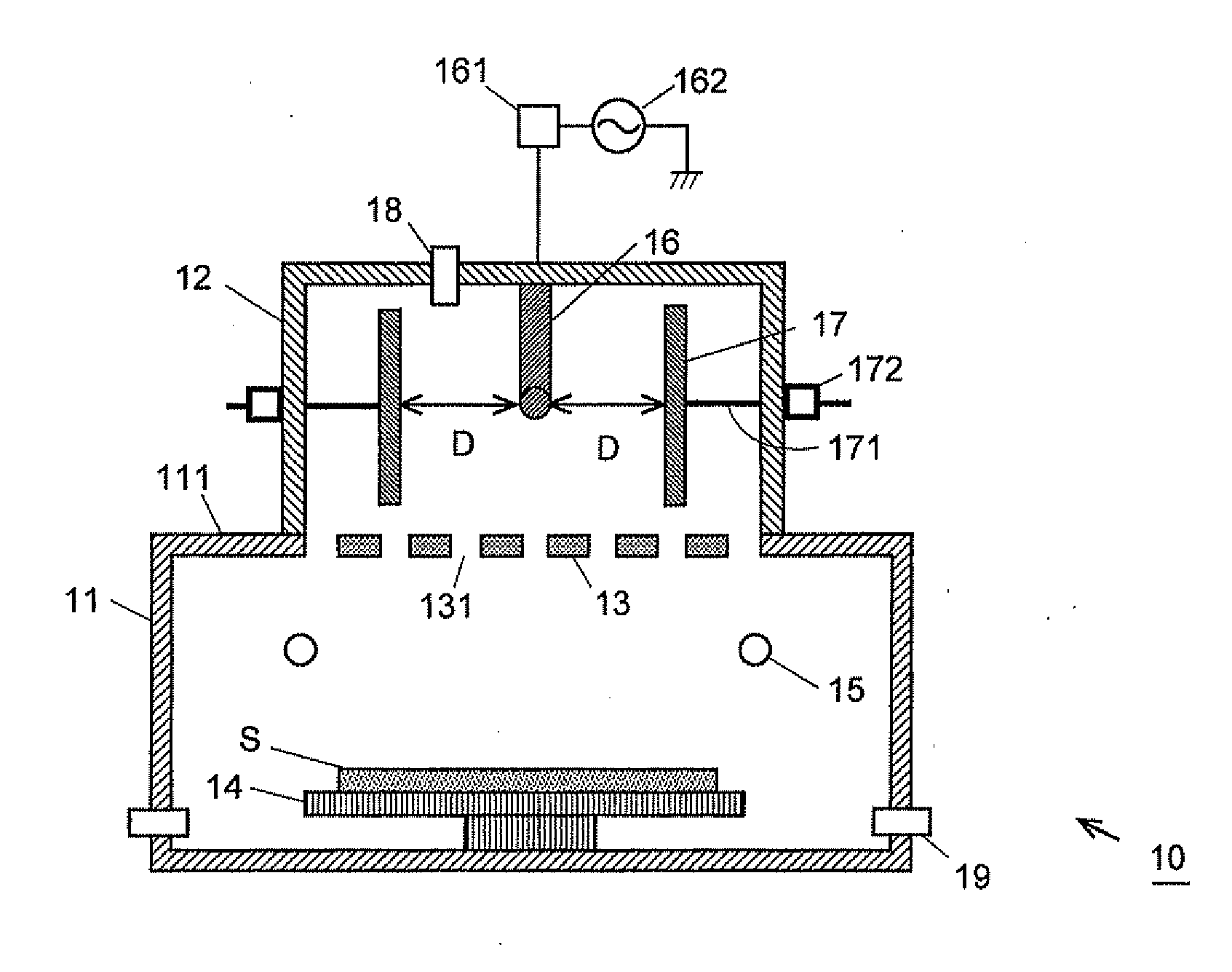
[0033]The first embodiment of the plasma processing device according to the present invention is schematically shown by a vertical sectional view in FIG. 4. The plasma processing device 10 of the present embodiment includes a plasma processing chamber 11 consisting of a rectangular parallelepiped vacuum container and a plasma producing chamber 12 which also consists of a rectangular parallelepiped vacuum container, the plasma producing chamber 12 being attached to the top panel (upper wall) 111 of the plasma processing chamber 11. A separation plate 13 having a large number of perforations 131 for generating a differential pressure between the plasma processing chamber 11 and the plasma producing chamber 12 is provided at the boundary between the plasma processing chamber 11 and the plasma producing chamber 12.

[0034]Inside the plasma processing chamber 11, a substrate table 14 on which a substrate S is to be placed is provided, facing the separation plate 13. The substrate table 14 ...

second embodiment

[0045]FIG. 6 is a vertical sectional schematic view of the second embodiment of the plasma processing device according to the present invention. The plasma processing device 20 of the present embodiment has the same structure as the plasma processing device 10 of the first embodiment except that a plurality of plasma producing chambers 22 are provided on the top panel 111 of one plasma processing chamber 11.

[0046]In the plasma processing 20 of the present embodiment, the energy of the electrons in the plasma in each of the plasma producing chambers 22 can be easily and individually controlled by independently adjusting the position of the plasma control plates 17 in each of the plasma producing chambers 22. By this system, the process can be controlled so that the deposition rate will be uniform over the entire substrate S. Accordingly, a highly uniform thin film can be produced even if the substrate has a large area. The state of plasma can be varied from one chamber to another; fo...

third embodiment

[0047]FIG. 7 is a vertical sectional schematic view of the third embodiment of the plasma processing device according to the present invention. The plasma processing device 30 of the present embodiment is a variation of the plasma processing device 20 of the second embodiment, in which an upper evacuation port 31 for discharging gas from the plasma processing chamber 11 is provided in the top panel 111 between each neighboring pair of the plasma processing chambers 22. Though not shown, a vacuum pump (evacuation system) and an evacuation rate regulator for regulating the evacuation rate of the vacuum pump are provided at each of the upper evacuation ports 31.

[0048]Normally, the evacuation of the plasma processing chamber 11 is performed through the evacuation ports (lower evacuation ports) 19 provided at a level lower than the substrate S. This is to prevent the processing gas for the film deposition from being excessively discharged. By contrast, in the plasma processing device 30 ...


PUM

PropertyMeasurementUnit
Pressureaaaaaaaaaa
Areaaaaaaaaaaa
Energyaaaaaaaaaa

Abstract

A plasma processing device according to the present invention includes a plasma processing chamber, a plasma producing chamber communicating with the plasma processing chamber, a radio-frequency antenna for producing plasma, a plasma control plate for controlling the energy of electrons in the plasma, as well as an operation rod and a moving mechanism for regulating the position of the plasma control plate. In this plasma processing device, the energy distribution of the electrons of the plasma produced in the plasma producing chamber can be controlled by regulating the distance between the radio-frequency antenna 16 and the plasma control plate by simply moving the operation rod in its longitudinal direction by the moving mechanism. Therefore, a plasma process suitable for the kind of gas molecules to be dissociated and/or their dissociation energy can be easily performed.

Description

TECHNICAL FIELD[0001]The present invention relates to a plasma processing device for performing a predetermined process, such as a deposition (film formation) or etching, on a substrate to be processed.BACKGROUND ART[0002]Plasma processing devices have been commonly used for the deposition of a thin film on a substrate, for the etching of a substrate and for other purposes. There are various types of plasma processing devices, such as a capacitively coupled type or inductively coupled type. Among those types, the inductively coupled plasma processing device is characterized by its capability of producing high-density plasma to perform a process at high speeds (for example, see Patent Document 1).[0003]A normal process of forming a silicon thin film by a plasma processing device is as follows: Initially, hydrogen gas (H2) and silane gas (SiH4) are introduced into a vacuum container, and an electric discharge power is supplied to produce plasma inside the vacuum container. In this pro...

Claims


Application Information

Patent Timeline
IPC IPC(8): H01L21/02H01L21/465
CPCC23C16/509H01J37/3211H05H1/46H01L21/465C23C16/24H01L21/02104H05H2001/4667H01J37/32357H01J37/32422H01J37/32568H01J37/32623H01J37/32834H01J37/32899H01J37/32954H05H1/4652H01L21/205H01L21/3065
Inventor SETSUHARA, YUICHIEBE, AKINORI
Owner ELECTRO-MOTIVE DIESEL
Why Eureka
Try Eureka