Thin film transistor, thin film transistor array substrate and method of fabricating the same

a thin film transistor and array substrate technology, applied in the direction of transistors, electroluminescent light sources, electric lighting sources, etc., can solve the problems of degenerating insulating characteristics, poor adhesion characteristics, and peeling of the insulating layer, so as to prevent a voltage drop problem, improve the effect of properties and improve the adhesion characteristics

Active Publication Date: 2013-08-15
LG DISPLAY CO LTD
View PDF3 Cites 11 Cited by
  • Summary
  • Abstract
  • Description
  • Claims
  • Application Information

AI Technical Summary

Benefits of technology

[0011]An object of the present invention is to provide an array substrate having improved properties.
[0012]Another object of the present invention is to provide a flat panel display device being capable of preventing a voltage drop problem by using a Cu layer, in particular, for the gate electrode.
[0013]Specifically, the present invention addresses the following objects. First, there is a problem of peeling of the insulating layer made of SiO2 from the gate electrode including Cu. This can be caused by a poor adhesion characteristics between SiO2 and Cu. This problem causes the diffusion of the Cu ion into the SiO2, which degenerates the insulating characteristics. Second, there is a problem of another peeling of the gate electrode including Cu from the substrate. This problem is caused also by the poor adhesion characteristics between the Cu and the substrate that is made of, for example, glass, plastic, and so on. Third, it is necessary to improve the resistance of the gate electrode including Cu against the oxide and H2O. Because, the Cu is easily subjected to the oxidation.

Problems solved by technology

First, there is a problem of peeling of the insulating layer made of SiO2 from the gate electrode including Cu.
This can be caused by a poor adhesion characteristics between SiO2 and Cu.
This problem causes the diffusion of the Cu ion into the SiO2, which degenerates the insulating characteristics.
Second, there is a problem of another peeling of the gate electrode including Cu from the substrate.
This problem is caused also by the poor adhesion characteristics between the Cu and the substrate that is made of, for example, glass, plastic, and so on.

Method used


Image

  • Thin film transistor, thin film transistor array substrate and method of fabricating the same
  • Thin film transistor, thin film transistor array substrate and method of fabricating the same
  • Thin film transistor, thin film transistor array substrate and method of fabricating the same

Examples


Embodiment Construction

[0026]Reference will now be made in detail to the embodiments, examples of which are illustrated in the accompanying drawings.

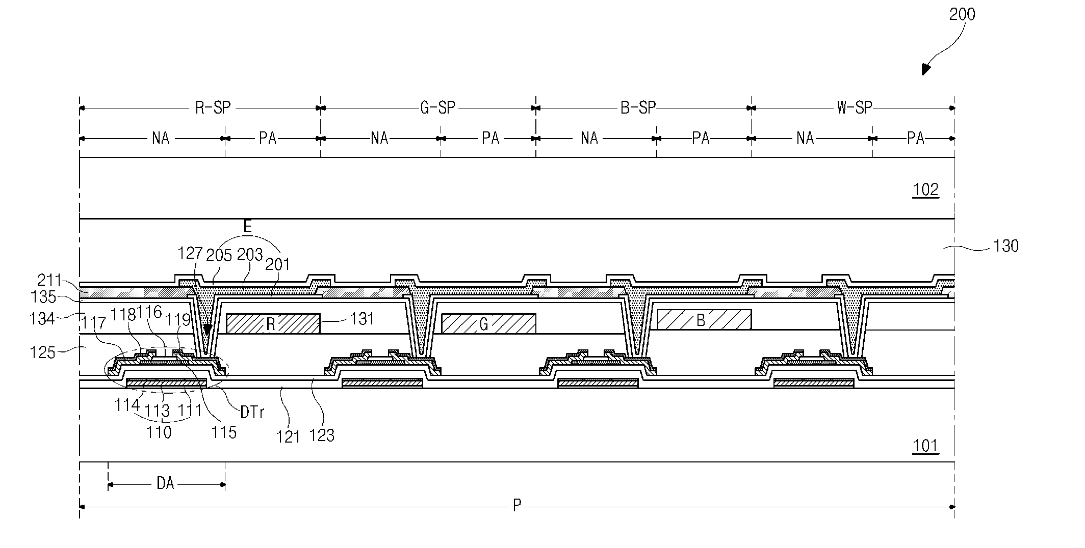
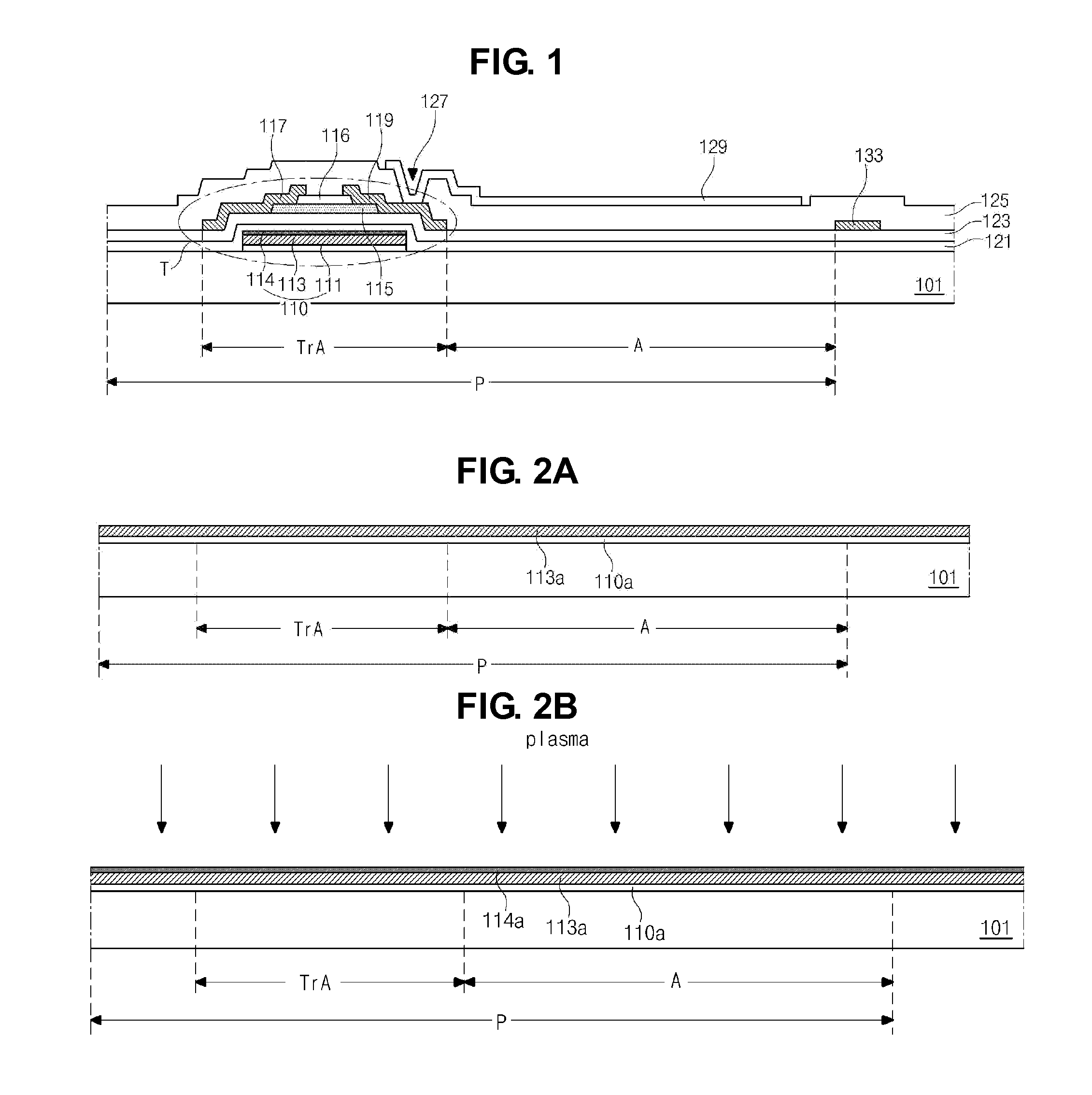
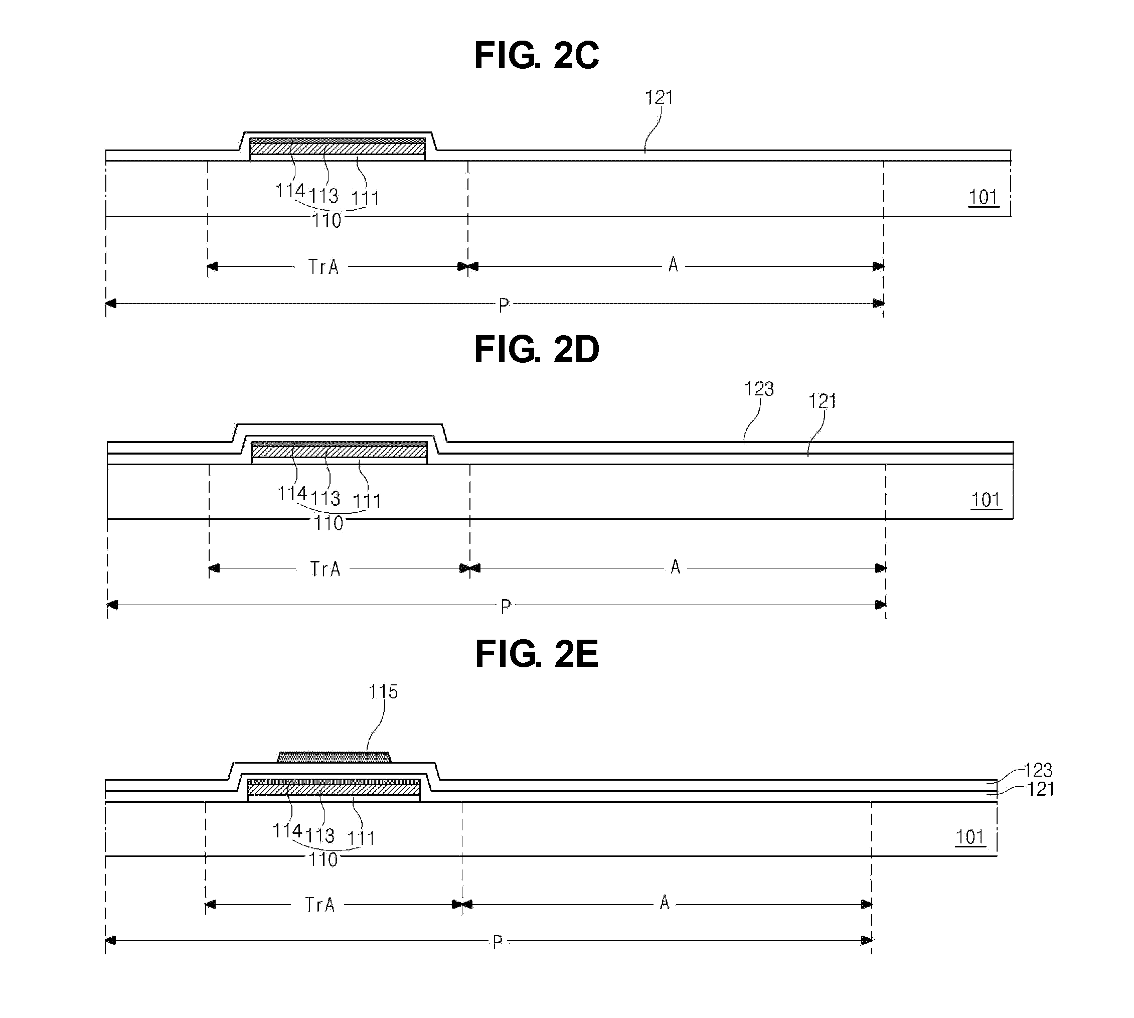
[0027]FIG. 1 is a cross-sectional view of an array substrate including a thin film transistor for a flat panel display device according to an embodiment of the present invention.

[0028]Referring to FIG. 1, an array substrate for a flat panel display device includes a gate line (not shown), a data line 133, a thin film transistor (TFT) T, a pixel electrode 129.

[0029]The gate line and the data line 133 cross each other to define a pixel region at a display region A. The TFT T is disposed at a crossing portion of the gate line and the data line 133. A region for the TFT T may be referred to as a switching region TrA. The pixel electrode 129 is disposed in the pixel region P.

[0030]The TFT T includes a gate electrode 110, a first gate insulating layer 121, a second gate insulating layer 123, an oxide semiconductor layer 115, a source electrode 117 and a drain elect...


PUM

PropertyMeasurementUnit
poweraaaaaaaaaa
poweraaaaaaaaaa
poweraaaaaaaaaa

Abstract

A method of fabricating a thin film transistor includes sequentially forming a first metal layer on a substrate and a second metal layer of copper on the first metal layer; performing a plasma process to form a copper nitride layer on the second metal layer; patterning the copper nitride layer, the second metal layer and the first metal layer to form a gate electrode; forming a first gate insulating layer of silicon nitride on the substrate including the gate electrode; forming a second gate insulating layer of silicon oxide on the first gate insulating layer; forming a semiconductor layer on the second gate insulating layer formed of an oxide semiconductor material; and forming a source electrode and a drain electrode on the semiconductor layer, the source electrode spaced apart from the drain electrode.

Description

[0001]The present application claims the benefit of Korean Patent Application No. 10-2012-0015290 filed in the Republic of Korea on Feb. 15, 2012, which is hereby incorporated by reference herein in its entirety.BACKGROUND OF THE INVENTION[0002]1. Field of the Invention[0003]The present invention generally relates to a thin film transistor (TFT) and a TFT array substrate, and more particularly to a TFT and a TFT array substrate using a copper signal line and a method of fabricating the same.[0004]2. Discussion of the Related Art[0005]A flat panel display device, for example, a plasma display panel (PDP) device, a liquid crystal display (LCD) device and an organic light emitting diode (OLED) device, is widely developed and used. Since the flat panel display device has advantages in thickness, weight and power consumption, it is used as a display device instead of the cathode ray tube (CRT).[0006]To meet requirements for a flat panel display device having a large size and high resolut...

Claims


Application Information

Patent Timeline
Patent Type & Authority Applications(United States)
IPC IPC(8): H01L29/786H01L29/66H05B44/00
CPCH01L29/786H01L29/66742H01L29/78693H01L29/45H01L29/4908H01L29/66969H01L27/124H01L29/7869
Inventor SEO, HYUN-SIKKIM, BONG-CHULKIM, DAE-WON
Owner LG DISPLAY CO LTD
Why Eureka
Try Eureka