Image sensor, camera, surveillance system, and method for driving the image sensor

a technology of image sensor and camera, which is applied in the direction of television system, television system scanning details, instruments, etc., can solve the problems of affecting the resolution increase, large circuit size of the pixel,

Active Publication Date: 2013-08-29
SEMICON ENERGY LAB CO LTD
View PDF12 Cites 65 Cited by
  • Summary
  • Abstract
  • Description
  • Claims
  • Application Information

AI Technical Summary

Benefits of technology

[0020]According to the invention disclosed in this specification, a difference in potential can be detected in a pixel without increase in the c

Problems solved by technology

However, when each pixel is provided with a circuit for difference calculation, such as a current mir

Method used


Image

  • Image sensor, camera, surveillance system, and method for driving the image sensor
  • Image sensor, camera, surveillance system, and method for driving the image sensor
  • Image sensor, camera, surveillance system, and method for driving the image sensor

Examples


embodiment 1

[0036]In this embodiment, an image sensor is described as an example of a semiconductor device with reference to FIG. 1, FIG. 2, FIG. 3, FIG. 4, FIG. 5, and FIG. 6.

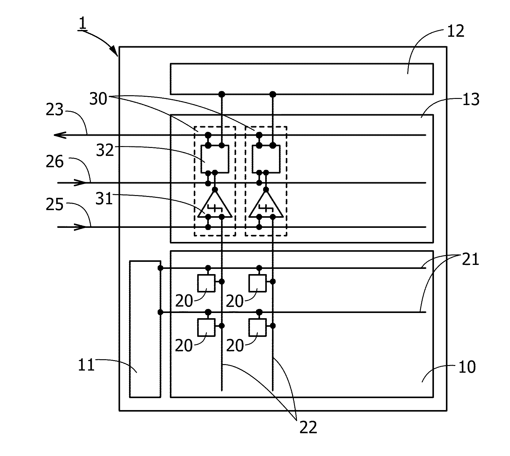
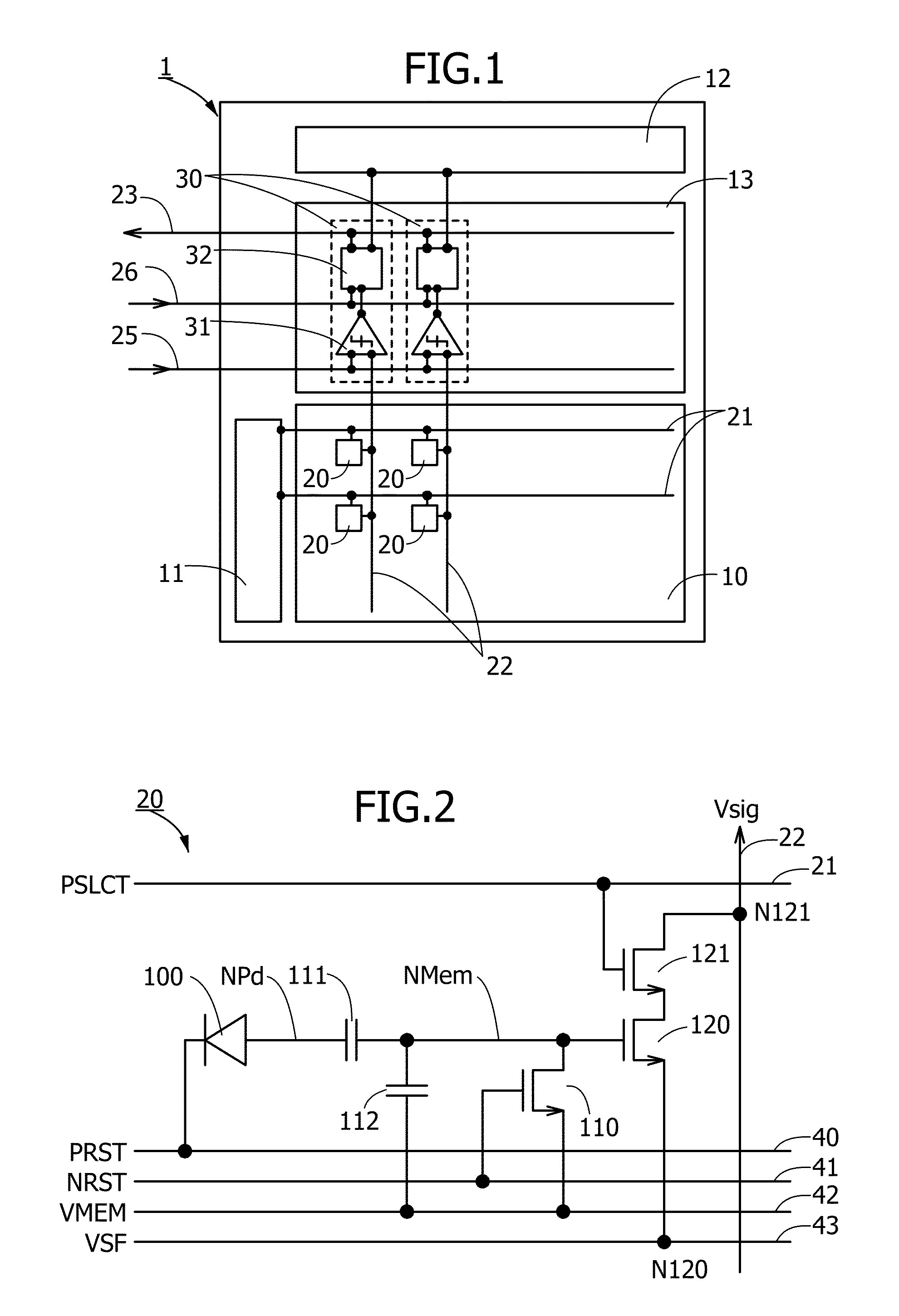
[0037]FIG. 1 illustrates an example of a configuration of an image sensor 1 of this embodiment. The image sensor 1 includes a pixel array 10, a vertical shift register 11, a horizontal shift register 12, and a reading circuit 13.

10>

[0038]The pixel array 10 includes a plurality of pixels 20, selection signal lines 21 each of which is provided per row, and vertical signal lines 22 each of which is provided per column. The pixels 20 are arranged two-dimensionally in a matrix. The pixels 20 at one row are electrically connected to the vertical shift register 11 through one selection signal line 21, and the pixels at one column are connected to the reading circuit 13 through one vertical signal line 22. The vertical shift register 11 is a circuit which controls scanning of the columns of the pixel array 10, and the selection s...

embodiment 2

[0098]In this embodiment, another configuration example of the pixel 20 is described. In this embodiment, a pixel for realizing an image sensor using a global shutter method is described with reference to FIG. 8 and FIG. 9.

50>

[0099]FIG. 8 is a circuit diagram illustrating an example of a configuration of a pixel 50 of this embodiment. The pixel 50 is different from the pixel 20 in that a switch for controlling electrical conduction between the photodiode 100 and the capacitor 111 is provided. In the pixel 50, a transistor 150 is provided as the switch. A gate of the transistor 150 is connected to a wiring 51, a source of the transistor 150 is connected to an output (an anode) of the photodiode 100, and a drain of the transistor 150 is connected to one electrode of the capacitor 111. The wiring 51 is a signal line to which a charge transmission control signal PTR (hereinafter referred to as a signal PTR) for controlling ON / OFF of the transistor 150 is input.

[0100]Note that although t...

embodiment 3

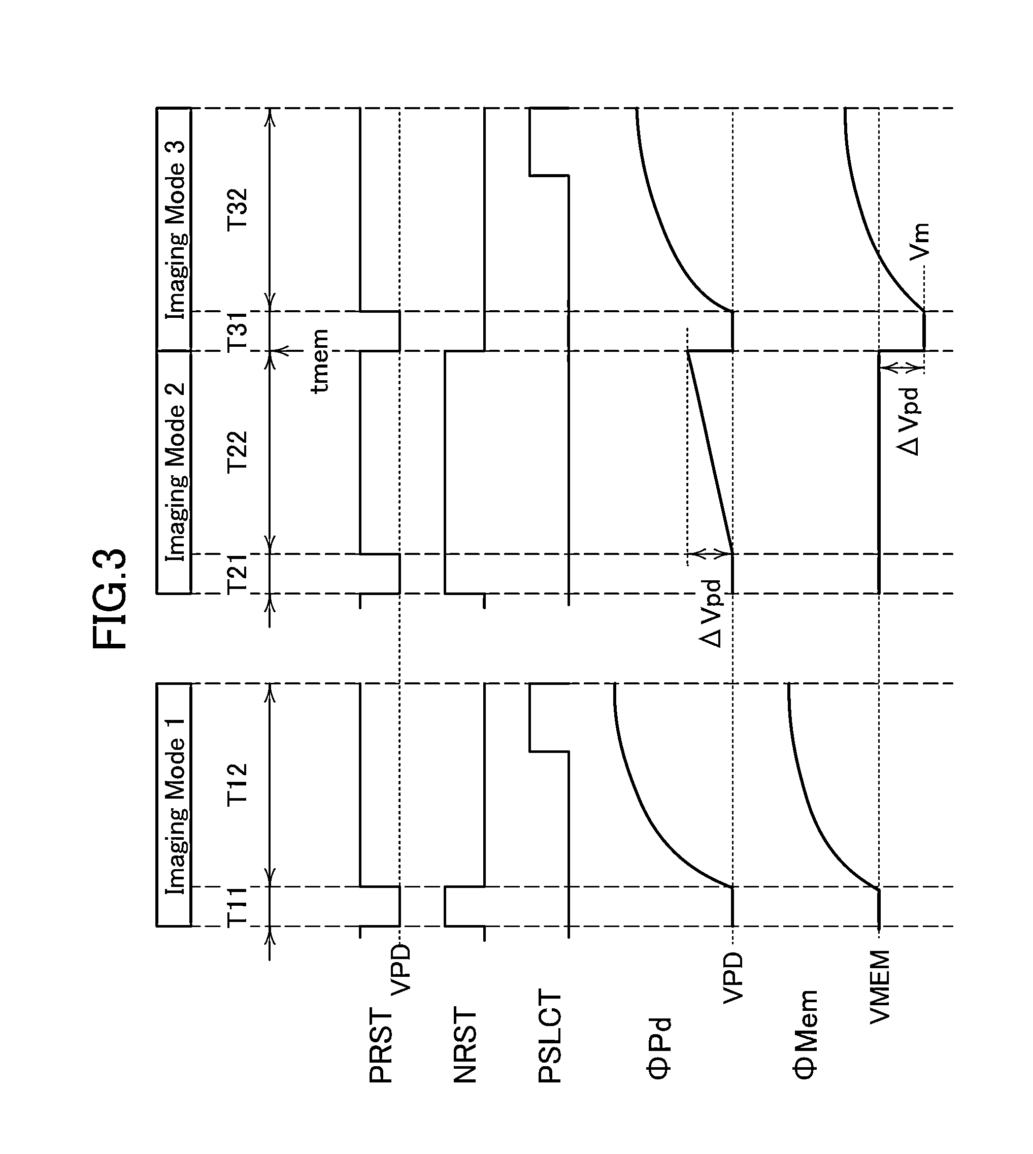
[0106]As described above, in the image sensor disclosed in this specification, each pixel can detect a difference in potential between optical signals in two different frames, and can detect a difference in potential between optical signals of not only successive two frames but two frames one of which is two or more frames before the other. Further, the detection accuracy of the difference in potential depends on the charge holding capability of the node (NMem) which functions as a memory of the potential memory circuit.

[0107]For example, in the pixel 20 where the leakage current of the transistor 110 at room temperature is approximately 1×10⁻¹⁴ A and the capacitance of the capacitor 112 is approximately 100 f F, when the frame rate is 60 fps, on the assumption that the potentials of the wirings other than the node NMem do not change, a period during which electric charge (potential) can be held at the node NMem is approximately one frame period ( 1 / 60 second).

[0108]Now, in this emb...


PUM


Abstract

Provided is an image sensor having a pixel includes a photoelectric conversion element; a capacitor which is connected between the photoelectric conversion element; a reset circuit which resets a potential of a node between the photoelectric conversion element and the capacitor; an amplifier circuit which outputs a signal corresponding to the potential of the node; and a switch which controls electrical conduction between the amplifier circuit and a vertical signal line. When the node is brought into an electrically floating state, the potential of the optical signal is stored in the node in a state of being inverted. When an optical signal is detected while the potential is stored in the node, the potential of the node increases in accordance with an output potential of the photoelectric conversion element, and thus the potential of the node corresponds to a difference in potential between the optical signals in different light-receiving periods.

Description

BACKGROUND OF THE INVENTION[0001]1. Field of the Invention[0002]The present invention relates to a product (including a machine, a manufacture, and a composition of matter) and a process (including a simple process and a production process). For example, in this specification, a semiconductor device, a method for driving the semiconductor device, a method for manufacturing the semiconductor device, and the like are described. In this specification, in particular, an imaging device including a photoelectric conversion element (e.g. an image sensor), a method for driving the imaging device, a camera including the imaging device, a surveillance system including the imaging device, and the like are described.[0003]A semiconductor device in this specification refers to any device that can function by utilizing semi conductor characteristics. A semi conductor circuit, an imaging device, an electro-optical device, a display device, a light-emitting device, an electronic device, and the lik...

Claims


Application Information

Patent Timeline
IPC IPC(8): H04N5/335H04N7/18H04N5/378H04N5/232
CPCH04N5/335H04N5/378H04N7/18H04N5/23254H04N23/6811H04N25/00H04N25/75H01L27/14609H01L27/14603H04N25/772
Inventor AOKI, TAKESHIIKEDA, TAKAYUKISATO, YURIKADAIRIKI, KOJI
Owner SEMICON ENERGY LAB CO LTD
Why Eureka
Try Eureka