

Piezoelectric device, method of manufacturing piezoelectric device, and liquid ejection head
- Summary
- Abstract
- Description
- Claims
- Application Information
AI Technical Summary
Benefits of technology
Problems solved by technology
Method used
Image

Examples
embodiment
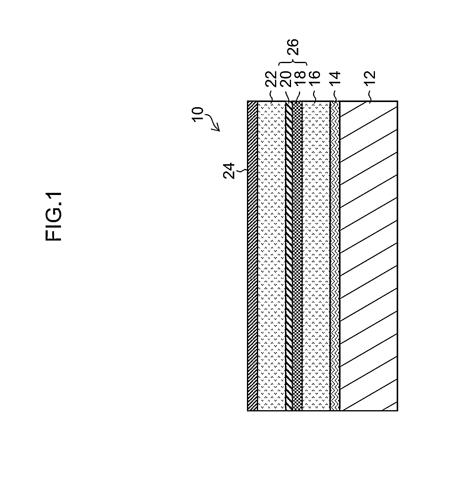
[0070]FIG. 1 is a cross sectional view showing a structure of a piezoelectric device according to an embodiment of the present invention. The piezoelectric device 10 shown in FIG. 1 has a laminated structure in which a first electrode 14 is formed on a substrate 12 functioning as a support body, a first piezoelectric film 16 is formed thereon, and a metal oxide film 18, a metal film 20, a second piezoelectric film 22 and a second electrode 24 are formed in layers further thereon in this order.
[0071]Here, in FIG. 1 and the other drawings, film thicknesses of the layers and a rate thereof are drawn while being appropriately changed for convenience of explanation, and are not necessarily shown by reflecting the actual film thicknesses and rate. Further, in the present specification, when describing the laminated structure, a direction of being away from the surface of the substrate 12 in a thickness direction of the substrate 12 is expressed as the “upper” direction. In FIG. 1, since t...
first practical example
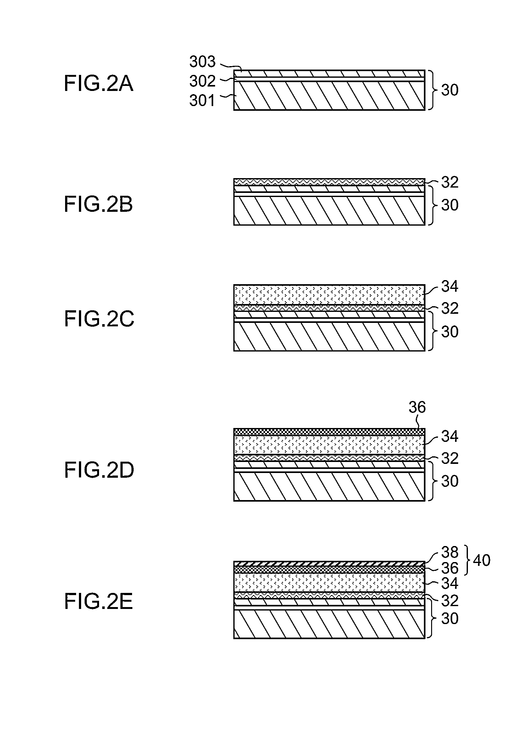
[0087]FIGS. 2A to 2I are views showing a manufacturing process of a piezoelectric device according to a first practical example of the present invention.
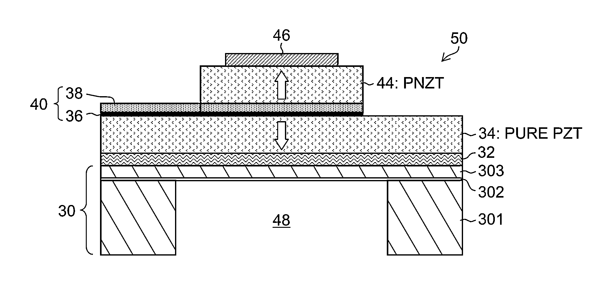
[0088]Step 1: First of all, a silicon-on-insulator (SOI) substrate 30 was prepared (FIG. 2A). The SOI substrate 30 has a laminated structure in which an Si layer 301 functioning as a handle layer, an oxide film layer (SiO2) layer 302 functioning as an insulating layer (a BOX layer) and an Si layer 303 functioning as a device layer are arranged. In place of the SOI substrate 30, a normal silicon substrate (an Si wafer) can be used.
[0089]Step 2: A film of TiW was formed at a film thickness of 20 nm on the Si layer 303 (the upper surface in FIG. 2B) of the SOI substrate 30 by means of the sputtering method, and a film of Ir was formed at a film thickness of 150 nm thereon. A lower electrode 32 was thereby formed to have a laminated structure of the TiW film of 20 nm and the Ir film of 150 nm.
[0090]Step 3: Thereafter, a film 34 of pure ...
second practical example
[0126]FIG. 7 is a schematic view of a device which is obtained according to a second practical example of the present invention. In FIG. 7, the same or similar elements as those in FIG. 5 are denoted with the same reference numerals, and description thereof is omitted.
[0127]In the second practical example, a device 70 similar to the device 50 obtained in the first practical example was prepared. In the second practical example, a piezoelectric film 74 of the first layer was composed of Nb doped PZT (PNZT), and a piezoelectric film 76 of the second layer was composed of the pure PZT. In other words, the PNZT film 74 in FIG. 7 had the same composition as the PNZT film 44 in FIG. 5, and the pure PZT film 76 in FIG. 7 had the same composition as the pure PZT film 34 in FIG. 5. The polarization process was carried out with respect to the pure PZT film 76 in the same manner as the first practical example, and the polarization state as shown with the outlined arrows in FIG. 7 was obtained....
PUM
| Property | Measurement | Unit |
|---|---|---|
| Thickness | aaaaa | aaaaa |
| Thickness | aaaaa | aaaaa |
| Pressure | aaaaa | aaaaa |
Abstract
Description
Claims
Application Information