Eureka AIR delivers breakthrough ideas for toughest innovation challenges, trusted by R&D personnel around the world.

Low resistance bidirectional junctions in wide bandgap semiconductor materials

Inactive Publication Date: 2013-10-17
CREE INC
View PDF8 Cites 48 Cited by
  • Summary
  • Abstract
  • Description
  • Claims
  • Application Information

AI Technical Summary

Benefits of technology

This patent is about a way to make a structure that reduces how much light is reflected at a specific wavelength. This is important because it can help improve the performance of the structure in applications like optical devices. The invention includes using a special layer with certain properties to achieve this. Additionally, the patent also mentions the use of certain impurities in a specific layer to further reduce the distance between different layers in the structure. This can help improve the performance of the structure even more.

Problems solved by technology

Unfortunately, there is an upper limit to how heavily a semiconductor material can be doped.
All dopants eventually reach a saturation solubility limit at which the material is no longer capable of absorbing further dopants without changing its composition.
Once this saturation limit is reached, doping loses its ability to reduce the tunnel width.
Furthermore, as the charge density increases the dopant ionization probability decreases according to basic semiconductor statistics, again limiting the ability of doping to reduce the tunnel width.
One difficulty with these nitride materials is that their band gap is significantly larger than the band gap of other III-V compound semiconductor materials (i.e., compound semiconductor materials including at least one element from column IIIA of the periodic table and at least one element from column VA of the periodic table).
A tunnel junction with low tunneling resistance is very difficult to form in wide band gap materials such as gallium nitride or silicon carbide.

Method used


Image

  • Low resistance bidirectional junctions in wide bandgap semiconductor materials
  • Low resistance bidirectional junctions in wide bandgap semiconductor materials
  • Low resistance bidirectional junctions in wide bandgap semiconductor materials

Examples


Embodiment Construction

[0058]Some embodiments of the invention provide non-rectifying conductive interfaces between p-type and n-type semiconductor layers. A non-rectifying conductive interface permits current to flow bidirectionally between the p-type and n-type layers, e.g., when a forward or reverse voltage is applied to the semiconductor layers.

[0059]Embodiments of the present invention now will be described more fully hereinafter with reference to the accompanying drawings, in which embodiments of the invention are shown. This invention may, however, be embodied in many different forms and should not be construed as limited to the embodiments set forth herein. Rather, these embodiments are provided so that this disclosure will be thorough and complete, and will fully convey the scope of the invention to those skilled in the art. Like numbers refer to like elements throughout.

[0060]It will be understood that, although the terms first, second, etc. may be used herein to describe various elements, these...


PUM


Abstract

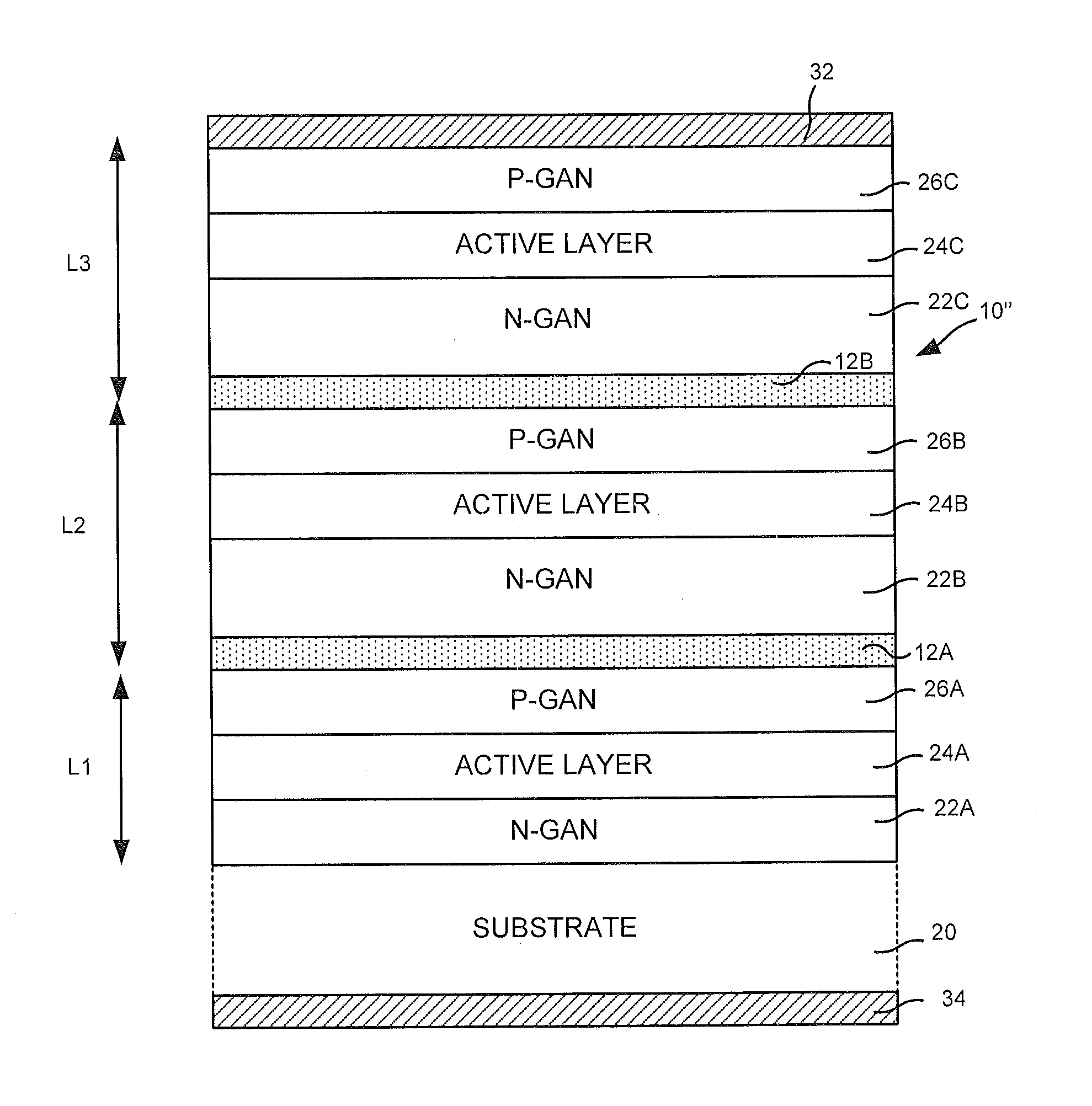
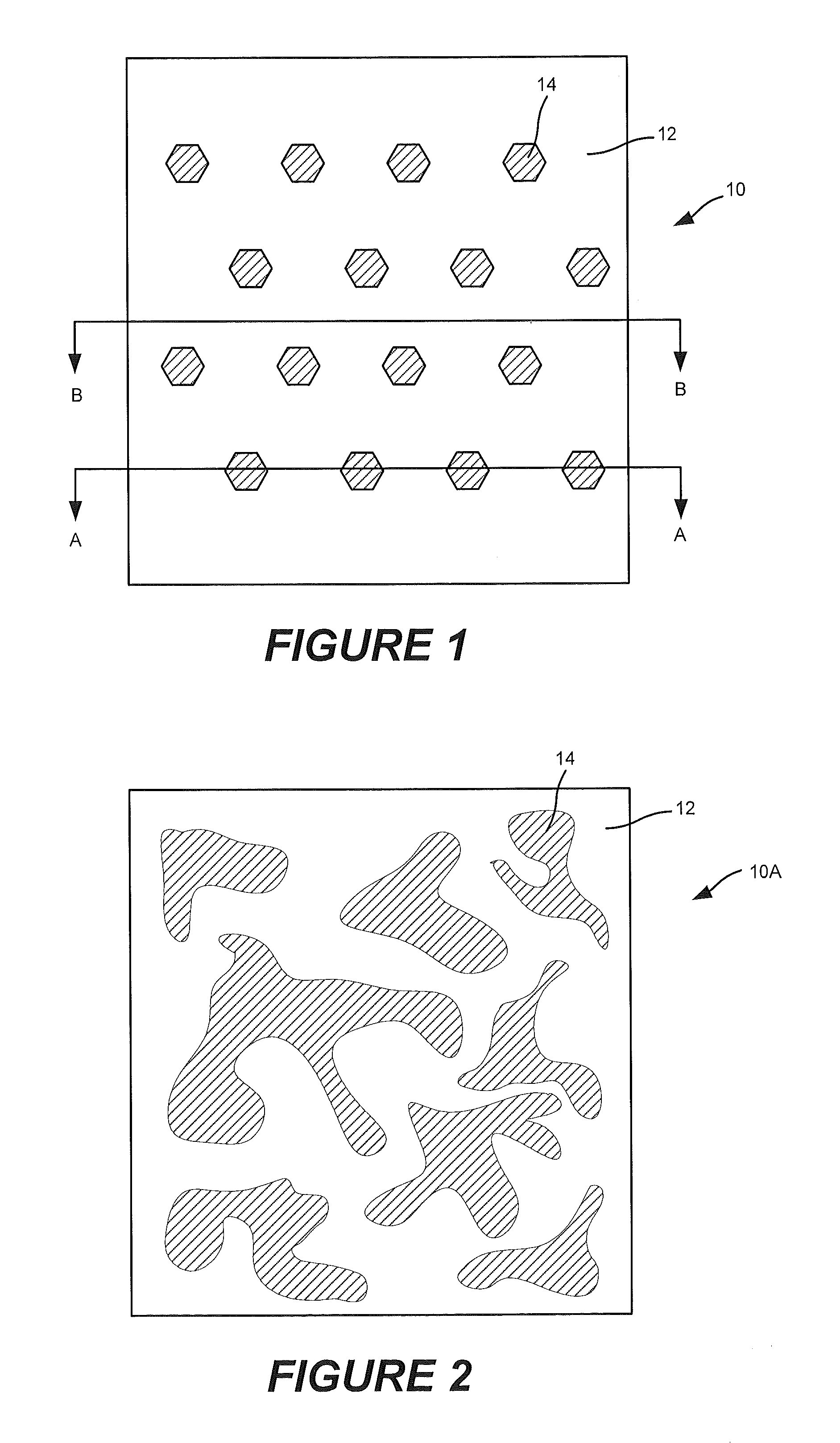
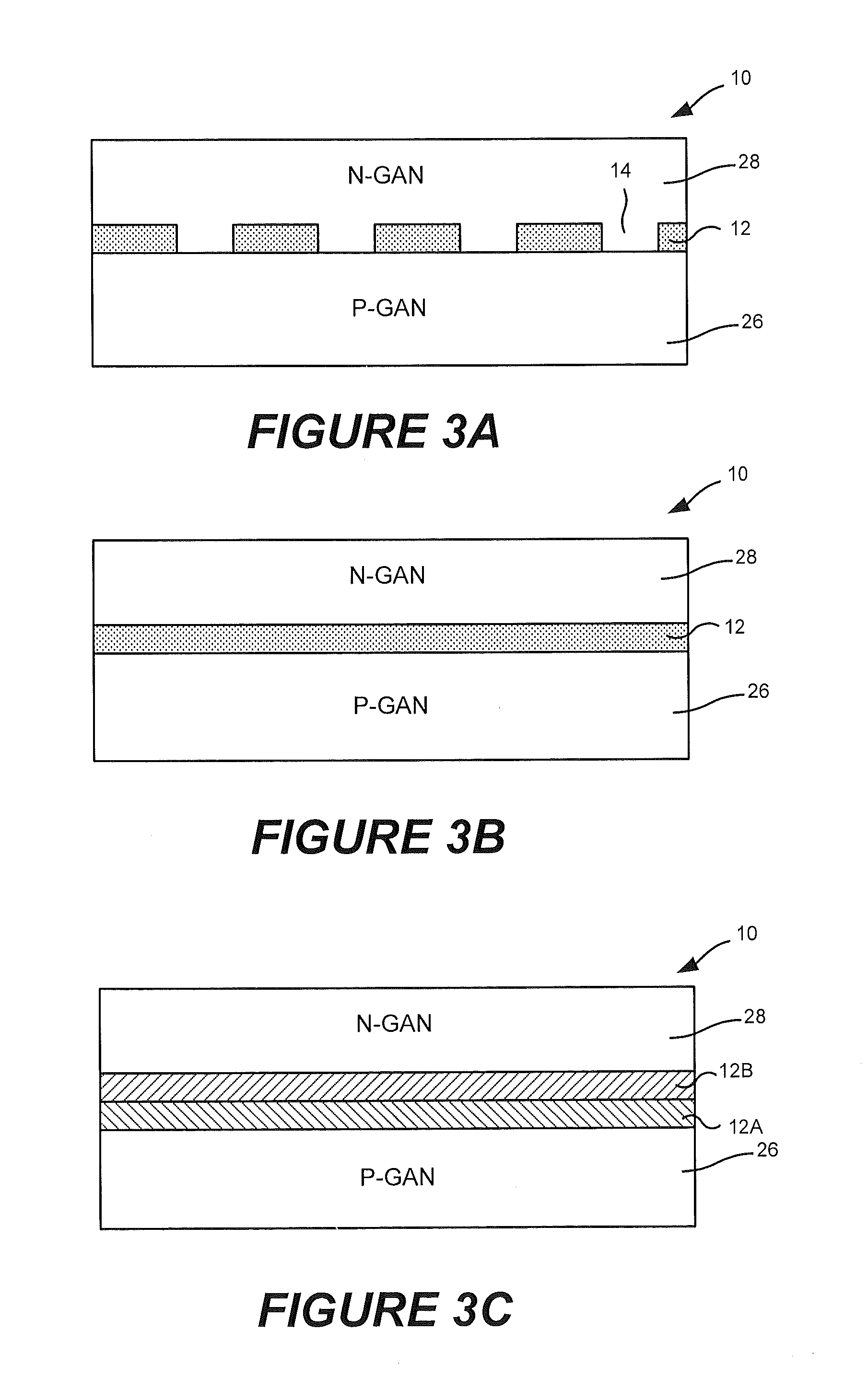
A light emitting diode device includes a first diode structure, a second diode structure on the first diode structure, and a conductive junction between the first diode structure and the second diode structure. The conductive junction includes a transparent conductive layer between the first diode structure and the second diode structure. Low resistance heterojunction tunnel junction structures including delta-doped layers are also disclosed.

Description

BACKGROUND[0001]1. Field of the Invention[0002]The present invention relates to semiconductor devices formed in wide band gap materials, and in particular to fabricating low resistance junctions in wide band gap materials.[0003]2. Description of the Related Art[0004]Semiconductor materials can be doped with impurities to be p-type materials in which positive charge carriers (e.g. holes) predominate or n-type materials in which negative charge carriers (e.g. electrons) predominate. Metallurgical junctions between differently doped regions of a single semiconductor material are called homojunctions. These junctions are formed, for example, when a single material abruptly transitions from one type of doping to another.[0005]A p-n junction consists of a p-type region and an n-type region in metallurgical contact with each other. When the p-type region and the n-type region comprise the same semiconductor material, the junction is referred to has a homojunction. Junctions between differe...

Claims


Application Information

Patent Timeline
IPC IPC(8): H01L33/06H01L29/38
CPCH01L29/861H01L29/868H01L29/2003H01L25/0756H01L33/08H01L33/42H01L2924/0002H01L2924/00
Inventor SAXLER, ADAM WILLIAM
Owner CREE INC
Why Eureka
Eureka Blog
Learn More