Driver for semiconductor switch element

a technology of semiconductor switch element and driver, which is applied in the direction of electronic switching, pulse generator, pulse technique, etc., can solve the problem that the transistor cannot be turned o

Inactive Publication Date: 2013-10-17
PANASONIC CORP
View PDF1 Cites 16 Cited by
  • Summary
  • Abstract
  • Description
  • Claims
  • Application Information

AI Technical Summary

Benefits of technology

[0029]The present invention can drive and turn-off a sem

Problems solved by technology

Therefore, in case where the FET is driven by the conventional driver having the circuit configuration shown in FIG. 17, there is a possi

Method used


Image

  • Driver for semiconductor switch element
  • Driver for semiconductor switch element
  • Driver for semiconductor switch element

Examples


first embodiment

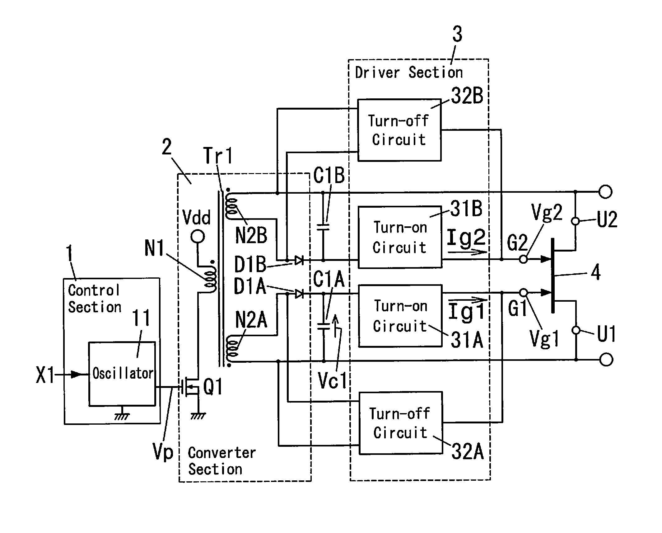
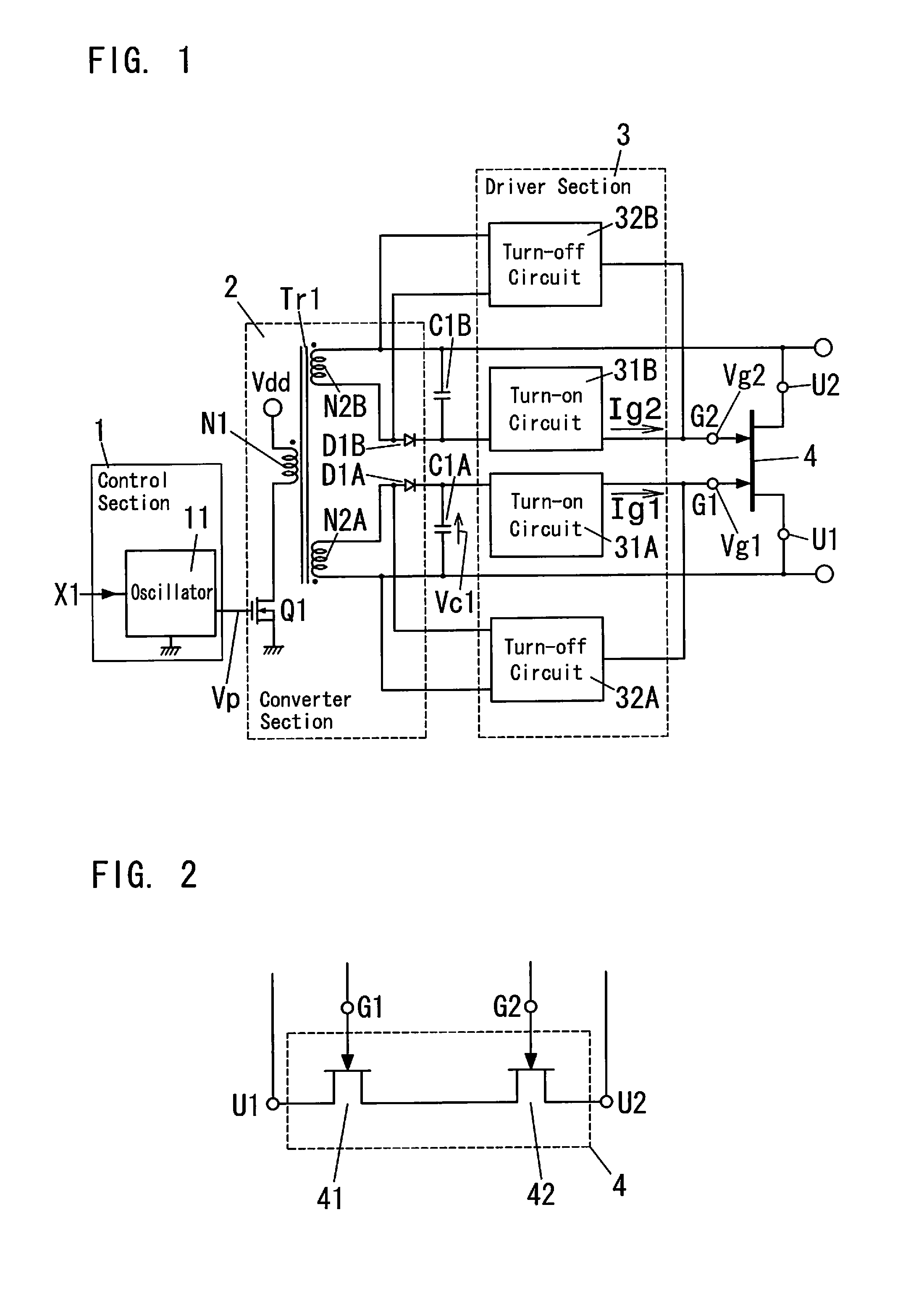
[0054]FIG. 1 shows a schematic configuration of a driver for semiconductor switch element according to the embodiment. The driver of the embodiment includes a control section 1, a converter section 2, a driver section 3, and capacitors C1A, C1B. The driver is configured to drive a bidirectional switch element 4 which is an example of the semiconductor switch element. The capacitors C1A, C1B serve as “a first capacitor” of the invention.

[0055]The bidirectional switch element 4 is a switching device that is formed of a wide-gap semiconductor having a large bandgap, such as SiC (silicon carbide) and GaN (gallium nitride). As shown in FIG. 2, the bidirectional switch element 4 is configured as a bidirectional switch formed of a pair of transistors 41, 42 that are connected in series, where each of the transistors 41, 42 has a gate, a source and a drain. In the bidirectional switch element 4, paths between the drain and the source of the transistors 41, 42 are respectively turned on (bec...

second embodiment

[0117]FIG. 13 shows a configuration of a control circuit (control section) 1 of the embodiment. The control circuit 1 includes an oscillator 12, a delay circuit 13, a D-A converter 14, and a comparator 15.

[0118]As shown in FIGS. 14A to 14E, the oscillator 12 outputs a signal X2 of a sinusoidal wave shape in response to the control signal X1 of H-level, to a non-inverting input terminal of the comparator 15. The delay circuit 13 outputs a delay signal X3, which is in L-level when receiving a control signal X1 of L-level and which is shifted from L-level to H-level upon elapse of a delay time Td after the shift of the control signal X1 from L-level to H-level. The D-A converter 14 outputs a threshold signal X4 (shown as a dotted-dash line in FIG. 14B), which is at “threshold voltage V4” when the delay signal X3 is in L-level and at “threshold voltage V5” when the delay signal X3 is in H-level. Note that, the threshold voltage V4 is larger than the threshold voltage V5.

[0119]The compar...

third embodiment

[0126]FIG. 18 shows a schematic configuration of a turn-on circuit 31 of the embodiment.

[0127]The turn-on circuit 31 of the embodiment includes: a constant current circuit 51 connected to a capacitor (first capacitor; forward capacitor) C1; and a noise-reduction circuit 52 connected to the constant current circuit 51. The noise-reduction circuit 52 of the embodiment includes: a capacitor (backward capacitor) C51; and a parallel circuit of a resistor (sixth resistor) R51 and a zener diode (second zener diode) ZD51. The capacitor C51 is connected in parallel with the capacitor C1 via the constant current circuit 51. The parallel circuit of the resistor R51 and the zener diode ZD51 is connected between an output terminal of the constant current circuit 51 and a gate G1 (G2) of the bidirectional switch element 4. In detail, a cathode of the zener diode ZD51 is connected to the output terminal of the constant current circuit 51 (and positive electrode of the capacitor C51), and an anode ...


PUM


Abstract

Providing a driver for semiconductor switch element capable of securing a sufficient drive power and reliably turning off the semiconductor switch element. The driver includes a converter section 2 which includes a switching element Q1 and which is configured to output a desired DC voltage by switching the switching element Q1, a control section 1 configured to control the switching operation of the switching element Q1, capacitors C1A, C1B charged by the output of the converter section 2, turn-on circuits 31A, 31B configured to supply gates of a bidirectional switch element 4 using electric charges stored in the capacitors C1A, C1B with drive powers to turn-on the bidirectional switch element 4, and turn-off circuits 32A, 32B configured to discharge the capacitors C1A, C1B to turn-off the bidirectional switch element 4 in response to the halt of the switching operation of the switching element Q1 by the control section 1.

Description

TECHNICAL FIELD[0001]The invention relates to a driver for semiconductor switch element.BACKGROUND ART[0002]There has been known a semiconductor switch element used as a switching element adapted in use for switching ON and OFF a power supply. Examples of the semiconductor switch elements include such as MOSFET (Metal Oxide Semiconductor Field Effect Transistor) and IGBT (Insulated Gate Bipolar Transistor).[0003]As a driver for driving the MOSFET or IGBT, there has been proposed to use an insulated type DC-DC converter with a transformer.[0004]For example, JP2003-69406A discloses an example of a driver for semiconductor switch element (see FIG. 17). In JP2003-69406A, a high voltage semiconductor switch is realized by a plurality of switching elements Q101 connected in series with each other, where each of the switching elements Q101 is constituted by IGBT. In the configuration of JP2003-69406A, diodes D101 are provided in inverse-parallel connections with the respective switching el...

Claims


Application Information

Patent Timeline
IPC IPC(8): H03K17/16
CPCH03K17/16H02M3/335H03K17/063H03K17/691H03K2017/066H03K2017/6878H03K2217/0081H03K17/163H02M1/08H02M3/22H02M3/24H02M3/28
Inventor HAYASHI, MASANORIHONDA, YOSHIAKIGOTOU, KIYOSHI
Owner PANASONIC CORP
Why Eureka
Try Eureka