

Charged particle beam apparatus
a charge particle and beam technology, applied in the direction of material analysis using wave/particle radiation, semiconductor/solid-state device testing/measurement, instruments, etc., can solve the problem of difficult observation which uses a charged particle beam having a high observation magnification at an initial stage, and achieve remarkable improvement in the wafer throughput.
- Summary
- Abstract
- Description
- Claims
- Application Information
AI Technical Summary
Benefits of technology
Problems solved by technology
Method used
Image

Examples
first embodiment
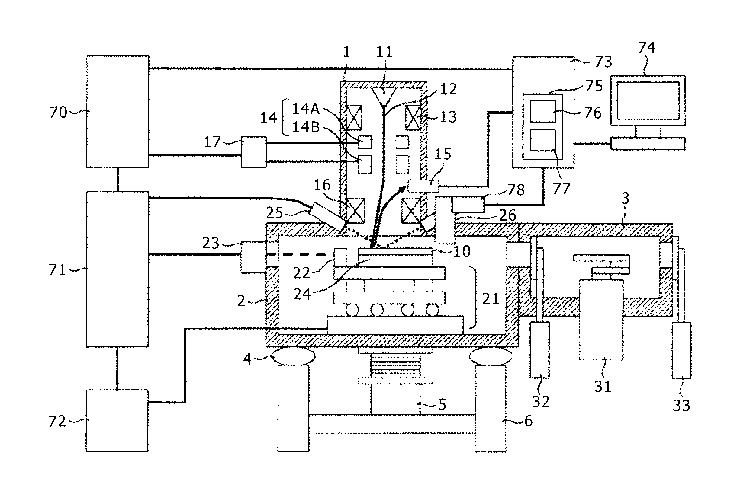
[0027]An explanation will be given of a configuration of a review SEM according to the present embodiment in reference to FIG. 1, FIG. 2, and FIG. 3.
[0028]First, an explanation will be given of an apparatus configuration shown in FIG. 1.
[0029]A frame 6 which is installed on a floor is attached with a mount 4 of removing a floor vibration, and the mount 5 supports a sample chamber 2. The sample chamber 2 is attached with a charged particle optical column 1 which generates a primary charged particle beam (primary electron beam in a case of the present embodiment), and focuses the primary charged particle beam onto a sample (hereinafter, abbreviated as column), and a load lock chamber 3 which incorporates a carrier robot 31 that carries the sample. The charged particle optical column 1 is attached with a secondary electron detector and a reflection electron detector, detects a secondary electron which is generated by primary electron irradiation or a reflection electron which is back-s...
second embodiment
[0079]According to the present embodiment, an explanation will be given of a configuration of a defect review SEM having a function of forming a focus map by removing an abnormal point. The total configuration of the apparatus and the outline operation flow are the same as those of the first embodiment, and therefore, the same explanation will be omitted in the following explanation and an explanation will be given only of a difference therefrom. Also, the drawings which are used in the first embodiment will be pertinently diverted.
[0080]As shown in FIG. 8, when a foreign matter is adhered to a back face of a reference wafer or an electrostatic chuck in forming a reference focus map, a locally raised shape is acquired. When an approximate polynomial is formed by a least squares method based on the result, a local change includes an error as if the focus map were raised at a periphery of the coordinate. (A maximum value becomes an error which is conversely pressed down) There are man...
third embodiment
[0088]An explanation will be given of a configuration of a defect review SEM including a function of monitoring an aging deterioration of a focus adjustment accuracy. Similar to the second embodiment, an explanation of a configuration and a function the same as those of the first embodiment will be omitted, and an explanation will be given only of a difference. Further, the drawings which are used in the first embodiment are pertinently diverted.
[0089]As described above, the focus control method which has been explained in the first embodiment resides in that the reproducibility with regard to the height direction is excellent, and the method is on the premise that there is not a relative variation with regard to heights of the Z sensor and the optical microscope. However, there is actually a variation in a temperature in a clean room at which a review SEM or other semiconductor inspection / measurement apparatus is installed, which has an influence on a focusing accuracy to no small ...
PUM
| Property | Measurement | Unit |
|---|---|---|
| thickness | aaaaa | aaaaa |
| thickness | aaaaa | aaaaa |
| time | aaaaa | aaaaa |
Abstract
Description
Claims
Application Information