Semiconductor device and method of manufacturing the same

a technology of semiconductors and semiconductors, applied in the direction of semiconductor devices, basic electric elements, electrical appliances, etc., can solve the problems of gate leakage current flowing, the performance of high electron mobility transistors to degrade, and the difficulty of reducing on-resistan

Inactive Publication Date: 2013-11-07
RENESAS ELECTRONICS CORP
View PDF6 Cites 31 Cited by
  • Summary
  • Abstract
  • Description
  • Claims
  • Application Information

AI Technical Summary

Benefits of technology

[0007]According to an embodiment, a high electron mobility transistor (field-effect transistor) includes a spacer layer between a channel layer and an electron supply layer, and a band gap of the spacer layer is larger than a band gap of the electron supply layer.

Problems solved by technology

That is, if the channel layer CH composed of gallium nitride (GaN) is formed directly on the semiconductor device 1S composed of silicon, a lot of crystal defects are formed in the channel layer CH, which causes the performance of the high electron mobility transistor to degrade.
The limitation of the maximum carrier concentration of the two-dimensional electron gas 2DEG means that the amount of carriers contributing as a channel current is limited, which makes it difficult to reduce the on-resistance.
It is thought that this results in the gate leakage current flowing from the gate electrode GE to the channel layer CH.

Method used


Image

  • Semiconductor device and method of manufacturing the same
  • Semiconductor device and method of manufacturing the same
  • Semiconductor device and method of manufacturing the same

Examples


first embodiment

Feature of First Embodiment

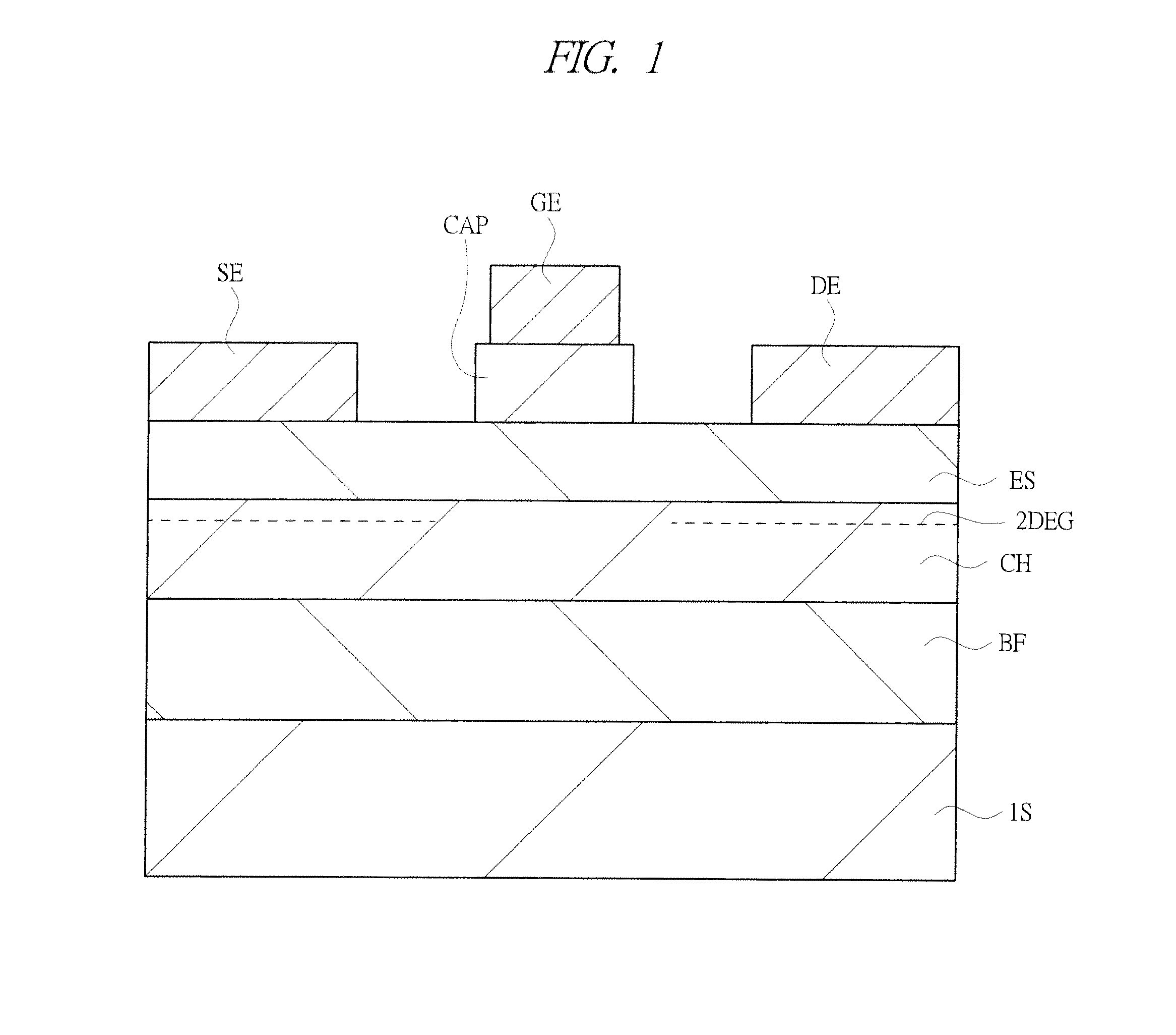
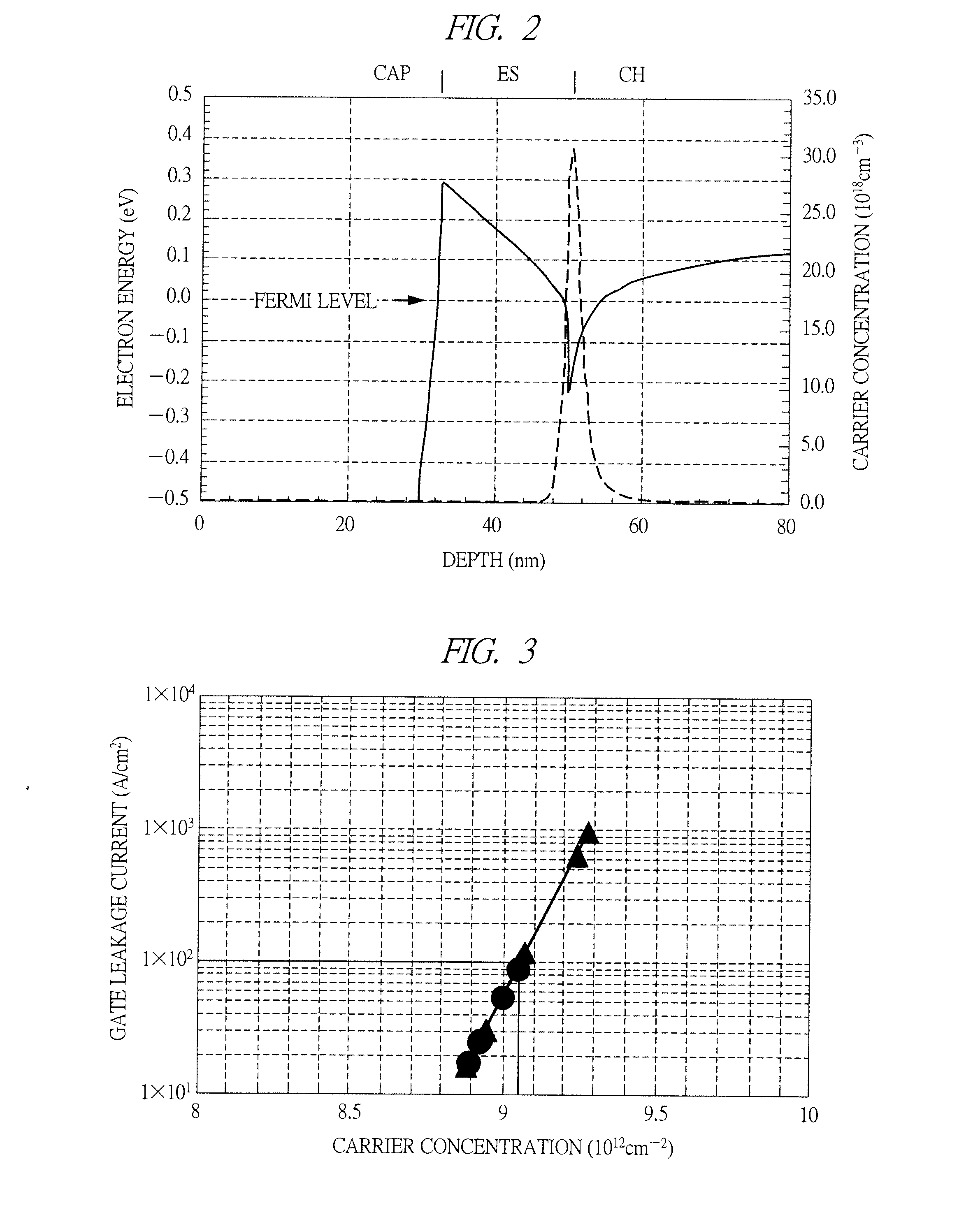
[0081]A feature in the first embodiment lies in that the spacer layer SP1 whose band gap is larger than the band gap of the electron supply layer ES1 is provided between the channel layer CH1 and the electron supply layer ES1, as shown in FIGS. 4 and 5. Thereby, due to the fact that the band gap of the spacer layer SP1 is large, a high potential barrier (electron barrier) is formed in the vicinity of the interface between the channel layer CH and the electron supply layer ES1. That is, a higher potential barrier is formed when the spacer layer SP1 is provided than when the spacer layer SP1 is not provided. As a result, according to the high electron mobility transistor in the first embodiment, the high potential barrier significantly suppresses the gate leakage current. Therefore, according to the high electron mobility transistor in the first embodiment, the maximum carrier concentration of the two-dimensional electron gas accumulated in the channel layer...

second embodiment

Feature of the Second Embodiment

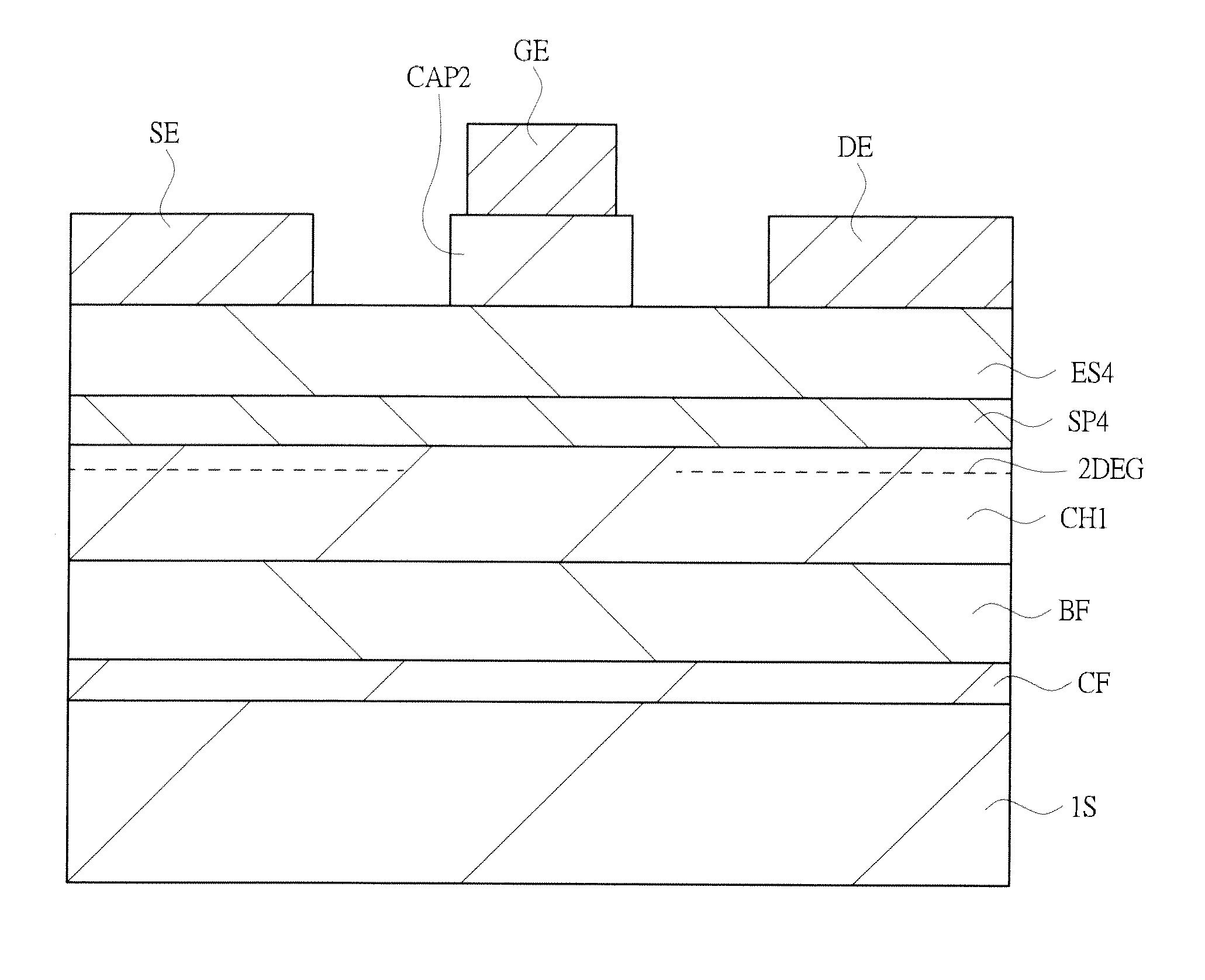
[0128]FIG. 18 is a sectional view showing the configuration of a high electron mobility transistor in a second embodiment. In FIG. 18, the same reference numerals as in FIG. 4 denote the same contents in FIG. 4, and the second embodiment differs from the first embodiment in the composition of a spacer layer SP2 and the composition of an electron supply layer ES2. That is, a feature of the second embodiment lies in that the spacer layer SP2 is composed of aluminum indium nitride (AluIn1-uN), and the electron supply layer ES2 is composed of aluminum gallium nitride (AlvGa1-vN).

[0129]Here, the band gap of the spacer layer SP2 composed of aluminum indium nitride (AluIn1-uN) is larger than the band gap of the electron supply layer ES2 composed of aluminum gallium nitride (AlvGa1-vN). Thereby, due to the fact that the band gap of the spacer layer SP2 is large, a high potential barrier (electron barrier) is formed in the vicinity of an interface between the ...

third embodiment

Feature of Third Embodiment

[0153]FIG. 23 is a sectional view showing the configuration of a high electron mobility transistor in a third embodiment. In FIG. 23, the same reference numerals as in FIG. 4 denote the same contents in FIG. 4, and the third embodiment differs from the first embodiment in the composition of a spacer layer SP3 and the composition of an electron supply layer ES3. That is, a feature of the third embodiment is that the spacer layer SP3 is composed of aluminum gallium nitride (AlaGa1-aN), and the electron supply layer ES3 is composed of aluminum indium nitride (AlbIn1-bN).

[0154]Here, the band gap of the spacer layer SP3 composed of aluminum gallium nitride (AlaGa1-aN) is larger than the band gap of the electron supply layer ES3 composed of aluminum indium nitride (AlbIn1-bN). Thereby, the fact that the band gap of the spacer layer SP3 is large, a high potential barrier (electron barrier) is formed in the vicinity of an interface between the channel layer CH1 an...


PUM


Abstract

In a high electron mobility transistor, with a normally-off operation maintained, on-resistance can be sufficiently reduced, so that the performance of a semiconductor device including the high electron mobility transistor is improved. Between a channel layer and an electron supply layer, a spacer layer whose band gap is larger than the band gap of the electron supply layer is provided. Thereby, due to the fact that the band gap of the spacer layer is large, a high potential barrier (electron barrier) is formed in the vicinity of an interface between the channel and the electron supply layer.

Description

CROSS-REFERENCE TO RELATED APPLICATION[0001]The present application claims priority from Japanese Patent Application No. 2012-105363 filed on May 2, 2012, the content of which is hereby incorporated by reference into this application.BACKGROUND[0002]The present invention relates to a semiconductor device and a technique of manufacturing the same, and, for example, relates to a technique effective when applied to a semiconductor device including a transistor using a nitride semiconductor and a technique of manufacturing the same.[0003]Japanese Patent Application Laid-Open No. H11-261053 (Patent Document 1), Japanese Patent Application Laid-Open No. 2005-244072 (Patent Document 2), and Japanese Patent Application Laid-Open No. 2006-339561 (Patent Document 3) describe techniques shown below, for example. That is, the above-mentioned documents describe a high electron mobility transistor (HEMT) provided with a channel layer, an electron supply layer formed on the channel layer, and a pa...

Claims


Application Information

Patent Timeline
Patent Type & Authority Applications(United States)
IPC IPC(8): H01L29/778H01L29/66
CPCH01L29/432H01L29/66462H01L29/7786H01L29/778H01L29/2003H01L29/205H01L29/1066H01L21/18
Inventor ANDO, YUJIOTA, KAZUKI
Owner RENESAS ELECTRONICS CORP
Why Eureka
Try Eureka