High temperature atomic layer deposition of silicon oxide thin films

Active Publication Date: 2013-11-07
VERSUM MATERIALS US LLC
View PDF4 Cites 315 Cited by
  • Summary
  • Abstract
  • Description
  • Claims
  • Application Information

AI Technical Summary

Benefits of technology

[0009]Described herein is a process for the deposition of a silicon oxide material or film at high temperatures, e

Problems solved by technology

However, the thermal oxidation process has a very low deposition rate, e.g., than 0.03 Å/s at 700° C. which makes it impractical for high volume manufacturing processes (see, for example, Wolf, S., “Silicon Processing for the VLSI Era Vol. 1—Process Technology”, Lattice Press, Calif., 1986).
However, silicon dioxide (SiO2) deposited at low temp

Method used


Image

  • High temperature atomic layer deposition of silicon oxide thin films
  • High temperature atomic layer deposition of silicon oxide thin films
  • High temperature atomic layer deposition of silicon oxide thin films

Examples


Example

Example 1

Atomic Layer Deposition of Silicon Oxide Films with Dimethylaminotrimethylsilane

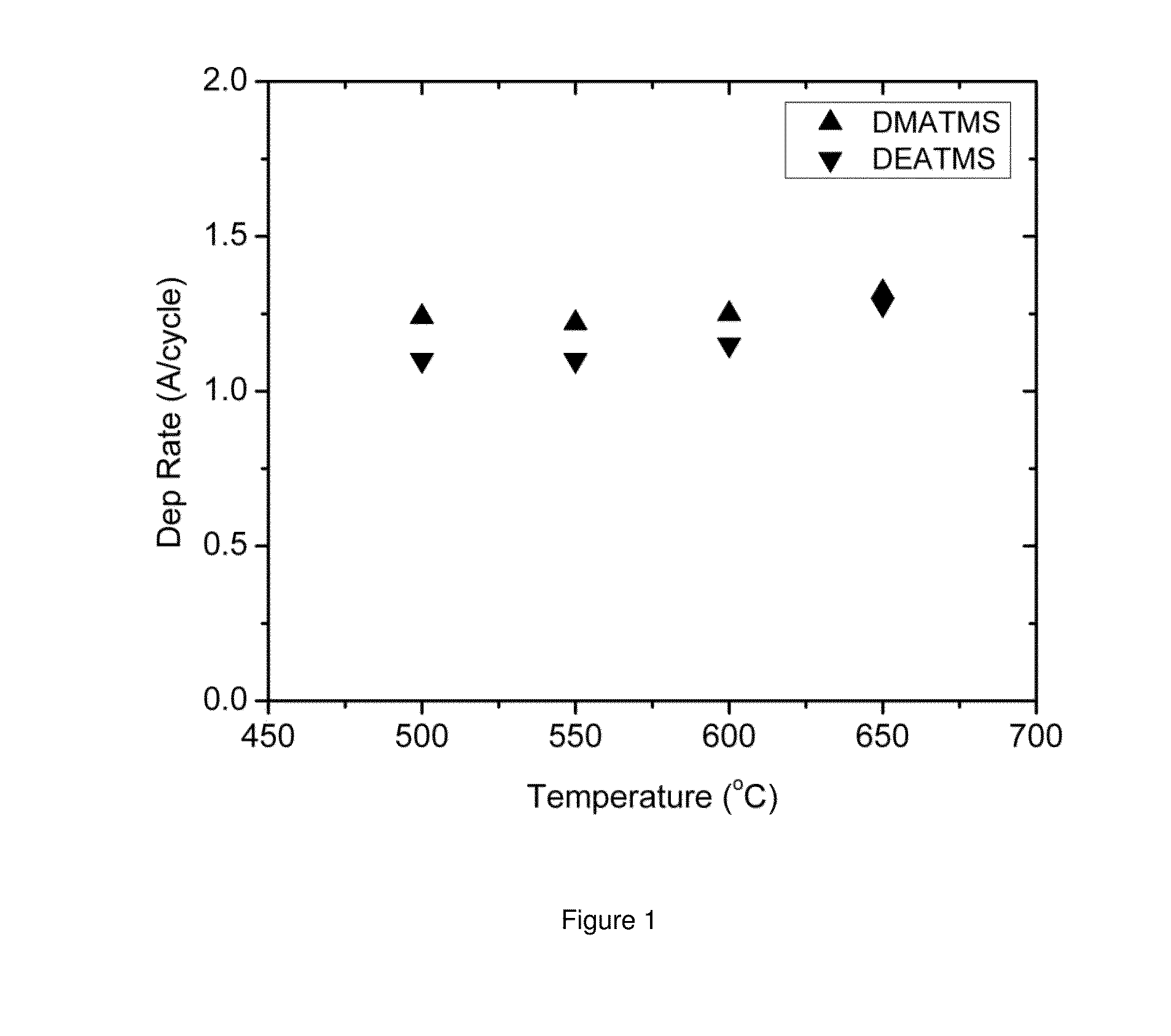
[0093]Atomic layer deposition of silicon oxide films were conducted using the following precursors: dimethylaminotrimethylsilane (DMATMS). The depositions were performed on a laboratory scale ALD processing tool. The silicon precursor was delivered to the chamber by vapor draw. All gases (e.g., purge and reactant gas or precursor and oxygen source) were preheated to 100° C. prior to entering the deposition zone. Gases and precursor flow rates were controlled with ALD diaphragm valves with high speed actuation. The substrates used in the deposition were 12 inch long silicon strips. A thermocouple attached on the sample holder to confirm substrate temperature. Depositions were performed using ozone as oxygen source gas. Deposition parameters are provided in Table I.

TABLE IProcess for Atomic Layer Deposition of SiliconOxide Films with Ozone Using DMATMSStep 16 secEvacuate reactorStep 2VariableDose ...

Example

Example 2

Atomic Layer Deposition of Silicon Oxide Films with Diethylaminotrimethylsilane

[0100]Atomic layer deposition of silicon oxide films were conducted diethylaminotrimethylsilane (DEATMS) using steps listed in Table I of Example 1. Deposition rate and film non-uniformity of SiO2 films deposited with DEATMS at 500-650° C. at a fixed precursor dose (8 seconds) are depicted in Table IV.

TABLE IVDeposition Rate and Film Non-Uniformity of SiO2 filmsdeposited with fixed DEATMS doseWaferDepositionNon-temperatureRateuniformity(Celcius)(Å / cycle)(%)5001.101.35501.101.06001.160.56501.272.5

[0101]To confirm ALD mode deposition, multiple precursor doses were used prior to ozone deposition steps to ensure the deposition is self-limiting. Deposition steps are listed Table V below:

TABLE VALD Conditions for Confirming ALD Mode Using DEATMSStep 16 secEvacuate reactorStep 2a2 secDose Silicon precursorReactor pressuretypically Step 2b2 secEvacuate reactorStep 36 secPurge reactor with nitrogenFlow 1....

Example

Example 3

Atomic Layer Deposition of Silicon Oxide Films on a Patterned Silicon Substrate with DMATMS

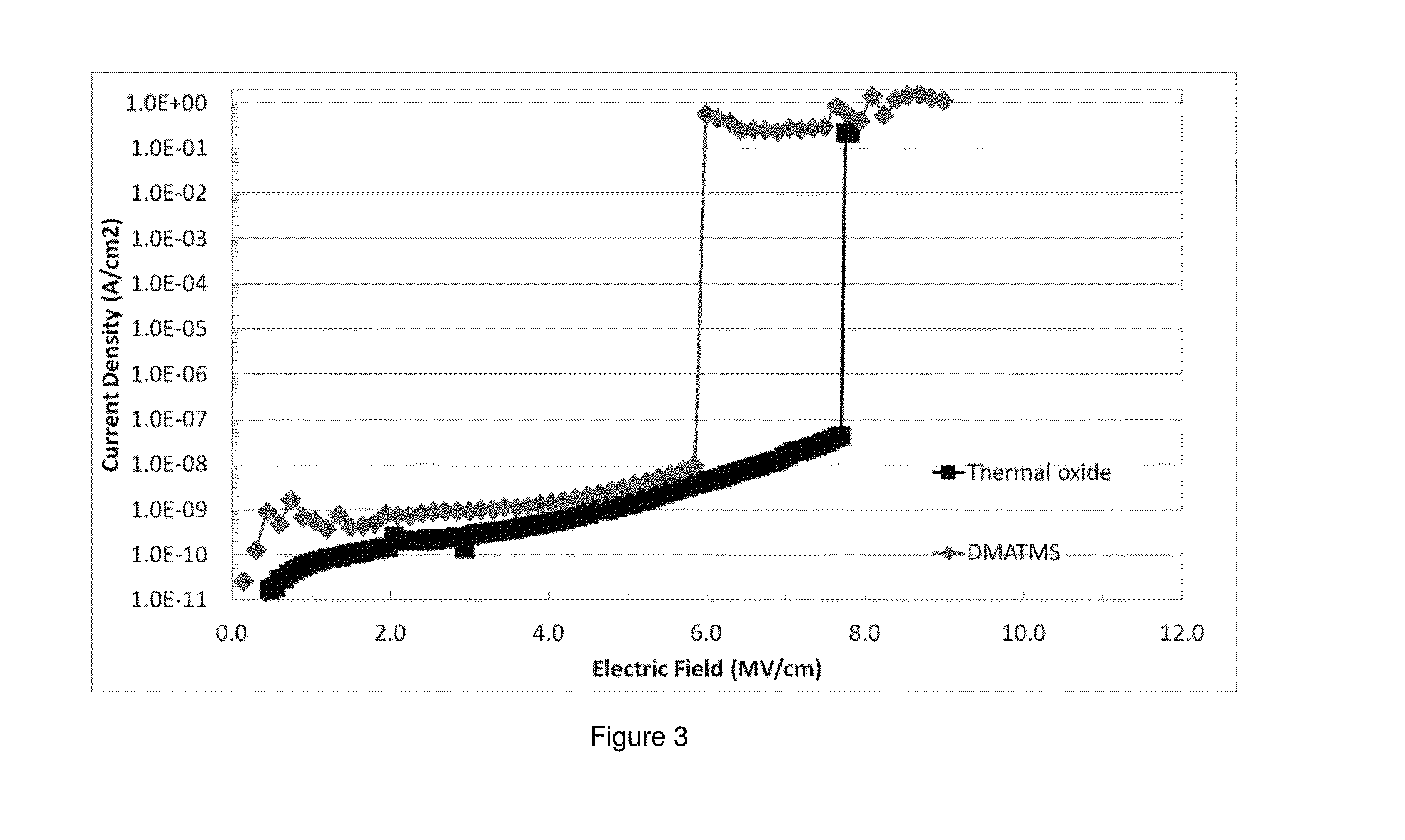
[0104]SiO2 film was deposited on patterned silicon wafers with DMATMS. The deposition process was performed using ozone as the oxygen source gas and precursor double pulse of 8 seconds at 650° C. The film deposited on the substrate was measured using field emission scanning electron microscopy (FESEM) Hitachi S-4800 SEM. The samples were mounted in cross-sectional holders and examined using SEM operated at 2 kV accelerating voltage. SiO2 thickness measurements of sample cross-sections were taken at the top, the side wall, and the bottom of the trench. A review of the SEM cross-section of the SiO2 film indicated excellent step coverage (>96%) and confirmed that the process is indeed an ALD process.


PUM

PropertyMeasurementUnit
Temperatureaaaaaaaaaa

Abstract

Composition(s) and atomic layer deposition (ALD) process(es) for the formation of a silicon oxide containing film at one or more deposition temperature of about 500° C. is disclosed. In one aspect, the composition and process use one or more silicon precursors selected from compounds having the following formulae I, II, described and combinations thereof
R1R2mSi(NR3R4)nXp; and  I.
R1R2mSi(OR3)n(OR4)qXp.  II

Description

CROSS REFERENCE TO RELATED APPLICATIONS[0001]This patent application claims the priority benefit of prior U.S. Provisional Patent Application Ser. No. 61 / 623,217 filed Apr. 12, 2012.BACKGROUND OF THE INVENTION[0002]Described herein is a composition and method for the formation of a silicon oxide film. More specifically, described herein is a composition and method for formation of a silicon oxide film at one or more deposition temperatures of about 500° C. or greater and using an atomic layer deposition (ALD) process.[0003]Thermal oxidation is a process commonly used to deposit high purity and highly conformal silicon oxide films such as silicon dioxide (SiO2) in semiconductor applications. However, the thermal oxidation process has a very low deposition rate, e.g., than 0.03 Å / s at 700° C. which makes it impractical for high volume manufacturing processes (see, for example, Wolf, S., “Silicon Processing for the VLSI Era Vol. 1—Process Technology”, Lattice Press, Calif., 1986).[0004...

Claims


Application Information

Patent Timeline
IPC IPC(8): H01L21/02
CPCH01L21/02164C23C16/402C23C16/45527C23C16/45553C07F7/10C23C16/448C23C16/45525C23C16/52H01L21/02274H01L21/0228
Inventor CHANDRA, HARIPINWANG, MEILIANGXIAO, MANCHAOLEI, XINJIANPEARLSTEIN, RONALD MARTINO'NEILL, MARK LEONARDHAN, BING
Owner VERSUM MATERIALS US LLC
Why Eureka
Try Eureka