
Circuit materials, multilayer circuits, and methods of manufacture thereof

Active Publication Date: 2008-10-16
WORLD PROPERTIES
View PDF14 Cites 21 Cited by
  • Summary
  • Abstract
  • Description
  • Claims
  • Application Information

AI Technical Summary

Benefits of technology

[0017]The circuit assemblies disclosed herein are capable of high temperature, lead-free processing. The circuit assemblies can be manufactured to be halogen-free, and yet flame-resistant and therefore can be used to form flame-resistant circuit materials having excellent electrical and physical properties.

Problems solved by technology

Thinner layers are desirable, but potentially increase dielectric or circuit related losses.
Lead-free solders meet this need, but require higher process temperatures that are harmful to multi-layer circuit materials having a high coefficient of thermal expansion (CTE) or low thermal stability.
However, these materials can have low melting points that limit the maximum use temperature or processing temperature of circuit assemblies.
Although high melting substrates simplify the fabrication of multi-layer circuits, other factors such as the substrate modulus can be limiting.
While there is a 35° C. temperature window between the melting points of this substrate and bond ply, the low modulus of the substrate at high temperature leads to distortion of the substrate during bonding.
This distortion causes poor registration between the layers of the circuit assembly.
On the other hand, if a substrate such as DuPont Teflon PFA film is used with a bond ply such as Ultralam® 3908, the 7° C. temperature window between the melting point of the substrate and that of the bond ply is too small to allow multi-layer circuits to be fabricated in an industrial process.
Multi-layer circuits made with PAEK substrates and FR4 epoxy (Tg=125° C.) cannot survive the high temperature required for lead-free soldering.
Such multi-layers also exhibit DF values that are too high for use in many high frequency devices.
Even with these improved properties of the thermosetting bonding ply, a circuit assembly made with this material and PAEK would not exhibit high performance.
The lead-free solder temperature resistance would not be high enough for robust manufacturing nor would the DF of the multi-layer assembly be low enough for many high frequency applications.

Method used


Image

  • Circuit materials, multilayer circuits, and methods of manufacture thereof
  • Circuit materials, multilayer circuits, and methods of manufacture thereof
  • Circuit materials, multilayer circuits, and methods of manufacture thereof

Examples


example 1

[0088]A 50.8 micrometer (2 mil) thick unfilled PEEK film from Ajedium Film Group, LLC (Newark, Del.) was melt laminated to ½ Oz MQ-VLP copper foil (Mitsui Mining and Smelting, Japan) to make double sided copper clad laminates. The material was laminated at 350° C. and 5.52 MPa (800 psi) for 45 minutes in an oil heated vacuum press. Some properties of these laminates are shown in Table 1.

example 2

[0089]A 50.8 micrometer (2 mil) thick 40 wt % talc polyether ether ketone film, Victrex® PEEK™ 450TL40, from Ajedium Film Group, LLC (Newark, Del.) was melt laminated to ½ Oz MQ-VLP copper foil (Mitsui Mining and Smelting, Japan) to make a double sided copper clad laminate. The material was laminated at 350° C. and 5.52 MPa (800 psi) for 45 minutes in an oil heated vacuum press. Some properties of this non-reinforced PEEK laminate are shown in Table 1. As shown in Table 1, the addition of the talc filler decreases the CTE and results in a significant improvement in the dimensional stability.

TABLE 1Unfilled PEEK40 wt % Talc FilledLaminatePEEK LaminatePropertyMDCMDZMDCMDZMechanical PropertiesDimensional Stability,−0.45−0.84N / A−0.20−0.24N / A% (Method B)Dimensional Stability,−0.37−0.83N / A−0.20−0.30N / A% (Method C)Copper Peel Strength,7.70 (4.4)7.35 (4.2)N / cm (pli)Thermal PropertiesCTE (30° C. to 150° C.),44.457.635.913.419.825.7ppm / ° C.Solder Resistance (60 sec),>330>365° C.Electrical Pro...

example 3

[0090]Two sheets of 50.8 micrometer (2 mil) thick unfilled PEEK film from Ajedium Film Group, LLC (Newark, Del.) were combined with on sheet of 1080 / 767 glass cloth (Hexcel Schwebel) in a hot oil vacuum press to make a melt laminated PEEK prepreg. This prepreg had a thickness of approximately 127 micrometer (5 mil) and was laminated at 350° C., 5.52 MPa (800 psi) for 60 minutes. A 50.8 micrometer (2 mil) PTFE release film was used on either side of the prepreg to prevent the PEEK from adhering to the stainless steel separator plates.


PUM

PropertyMeasurementUnit
Temperatureaaaaaaaaaa

Abstract

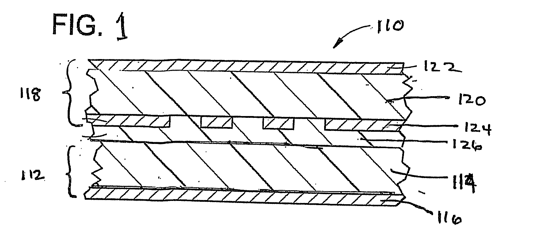
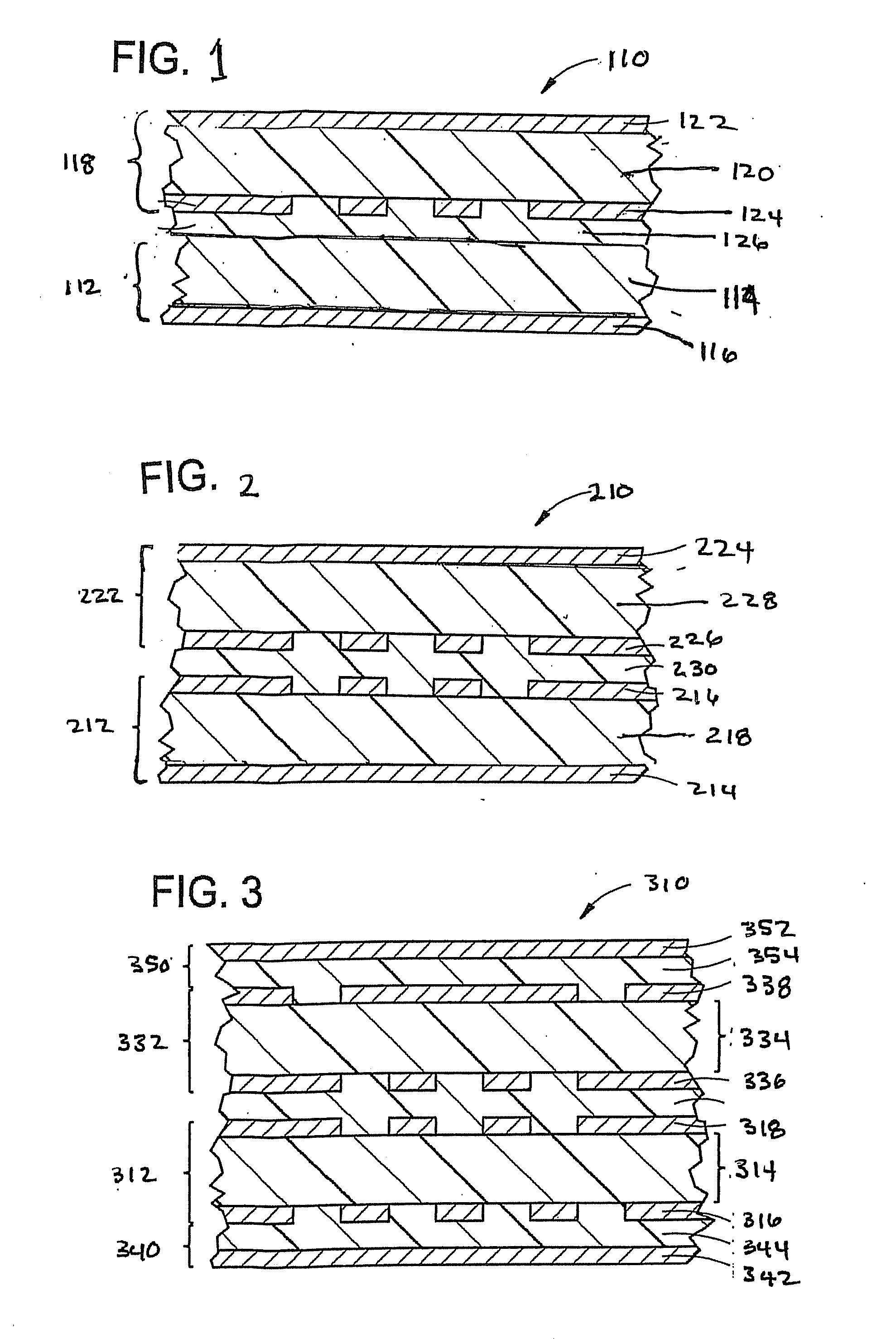
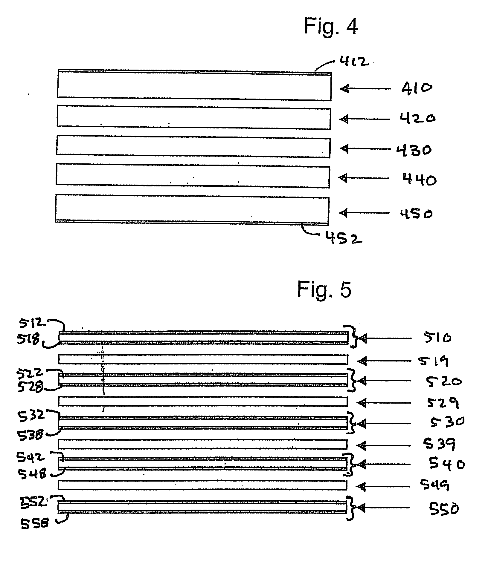
A circuit assembly comprises two or more circuit laminates, each comprising a conductive metal layer disposed on a poly(arylene ether ketone) substrate layer, wherein at least one of the conductive metal layers has been patterned to form a circuit, and a bond ply layer comprising a thermoplastic or thermosetting material. The thermoplastic bond ply has a melting point between 250° C. and 370° C., a decomposition temperature greater than about 290° C. and a dissipation factor of less than 0.01 at 10 GHz. The thermoset bond ply has a dissipation factor less than 0.01 at 10 GHz and a decomposition temperature greater than about 290° C. after lamination. Methods of forming the above circuit assemblies are also disclosed.

Description

CROSS-REFERENCE TO RELATED APPLICATION[0001]This application claims the benefit of U.S. Provisional Application No. 60 / 911,164, filed Apr. 11, 2007, which is incorporated by reference herein in its entirety.BACKGROUND OF INVENTION[0002]This invention relates to materials and methods for the manufacture of circuit materials and multilayer circuits.[0003]Printed circuit boards must meet increasingly stringent performance and environmental requirements. For example, advanced printed circuit boards incorporate more layers and operate at increasingly higher frequencies. Thinner layers are desirable, but potentially increase dielectric or circuit related losses. To meet this need, substrates that have a dielectric constant (Dk) less than 4 can be used, as such substrates can accommodate higher signal propagation speeds, while minimizing insertion loss.[0004]For environmental reasons, manufacturers seek to reduce heavy metals in circuit assemblies. Lead-free solders meet this need, but req...

Claims


Application Information

Patent Timeline
IPC IPC(8): H01L29/12H05K3/20
CPCH05K3/4611H05K3/4626H05K2201/0129H05K2201/0141Y10T29/49128H05K2201/0209Y10T428/24917Y10T428/12528H05K2201/015
Inventor KENNEDY, SCOTT D.LANDI, VINCENT R.WHITE, MICHAEL S.NAVARRO, DANIEL J.MAGREY, DONALD P.
Owner WORLD PROPERTIES
Learn More