Silicon carbide semiconductor device and manufacturing method thereof

Inactive Publication Date: 2007-10-18
FUJI ELECTRIC HLDG CO LTD
View PDF0 Cites 18 Cited by
  • Summary
  • Abstract
  • Description
  • Claims
  • Application Information

AI Technical Summary

Benefits of technology

[0041]By the second method according to the invention, Si atoms diffusing in the oxide force carbon impurities or suboxides to be spent. Furthermore, as opposed to the first method, the second method has an advantage of necessitating no such abnormally high temperature as to make SiO2 in a liquefied state including no crystalline materials. Furthermore, the first method also has the effect as explained below when applied to the case of formin

Problems solved by technology

It is reported that a high breakdown voltage power device fabricated by using a silicon carbide (SiC) semiconductor substrate has a possibility of considerably lowering on-resistance of the device.
At present, although on-resistance can be lowered, the extent of the lowering is insufficient, and there exists a desire for even further lowering.
Moreover, excessive thermal oxidation of SiC causes suboxides or carbon clusters at a MOS interface to increase as in the case of forming a thermal oxidation film.
This results in an increase in an interface state density to decrease MOS channel mobility.
However, it is additionally reported that carbon atoms are actually almost impossible to move in SiO2 in a non-oxidizing atmosphere even by heating, and that oxidation of carbon in an

Method used


Image

  • Silicon carbide semiconductor device and manufacturing method thereof
  • Silicon carbide semiconductor device and manufacturing method thereof
  • Silicon carbide semiconductor device and manufacturing method thereof

Examples


Example

Example 1

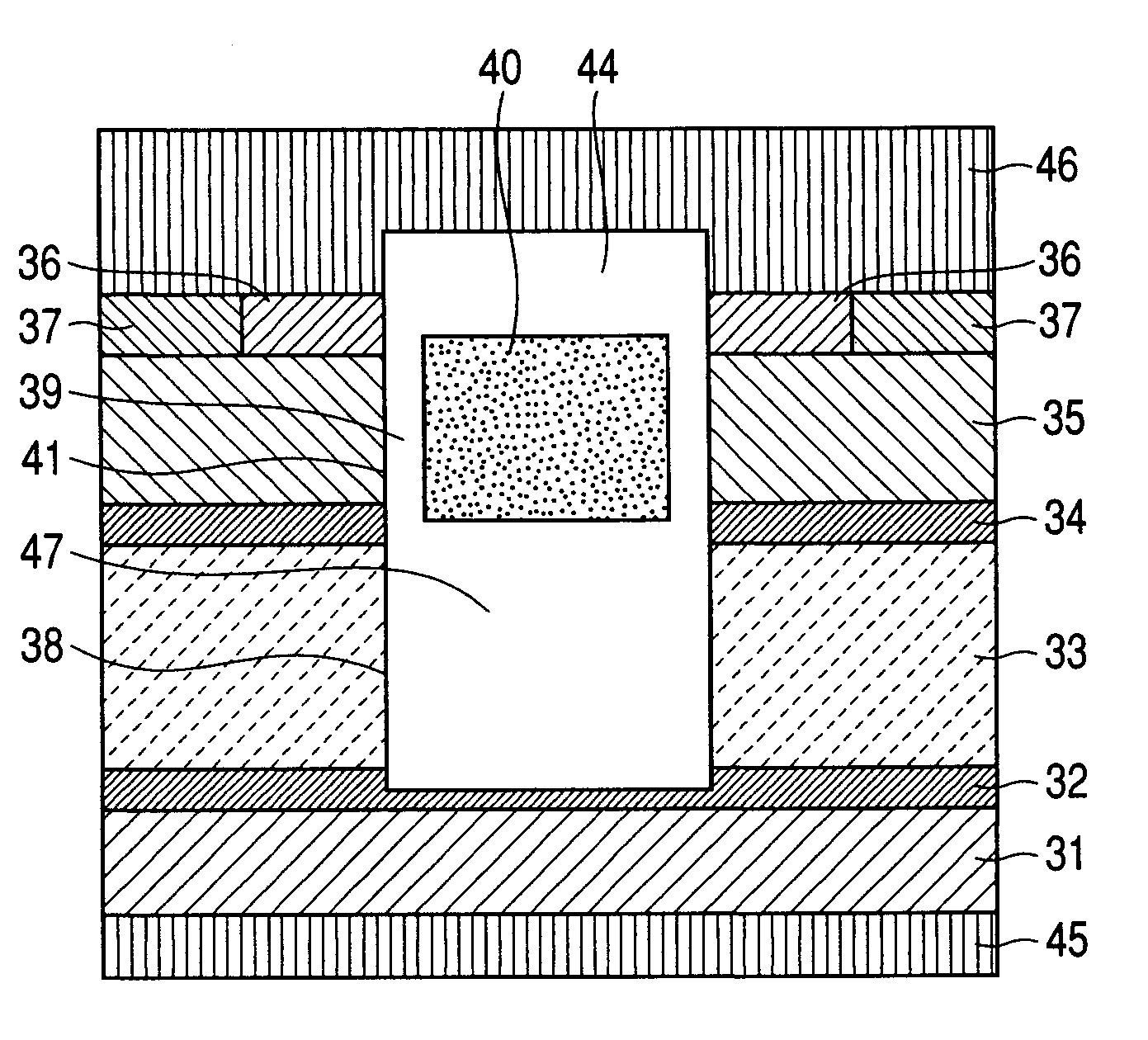
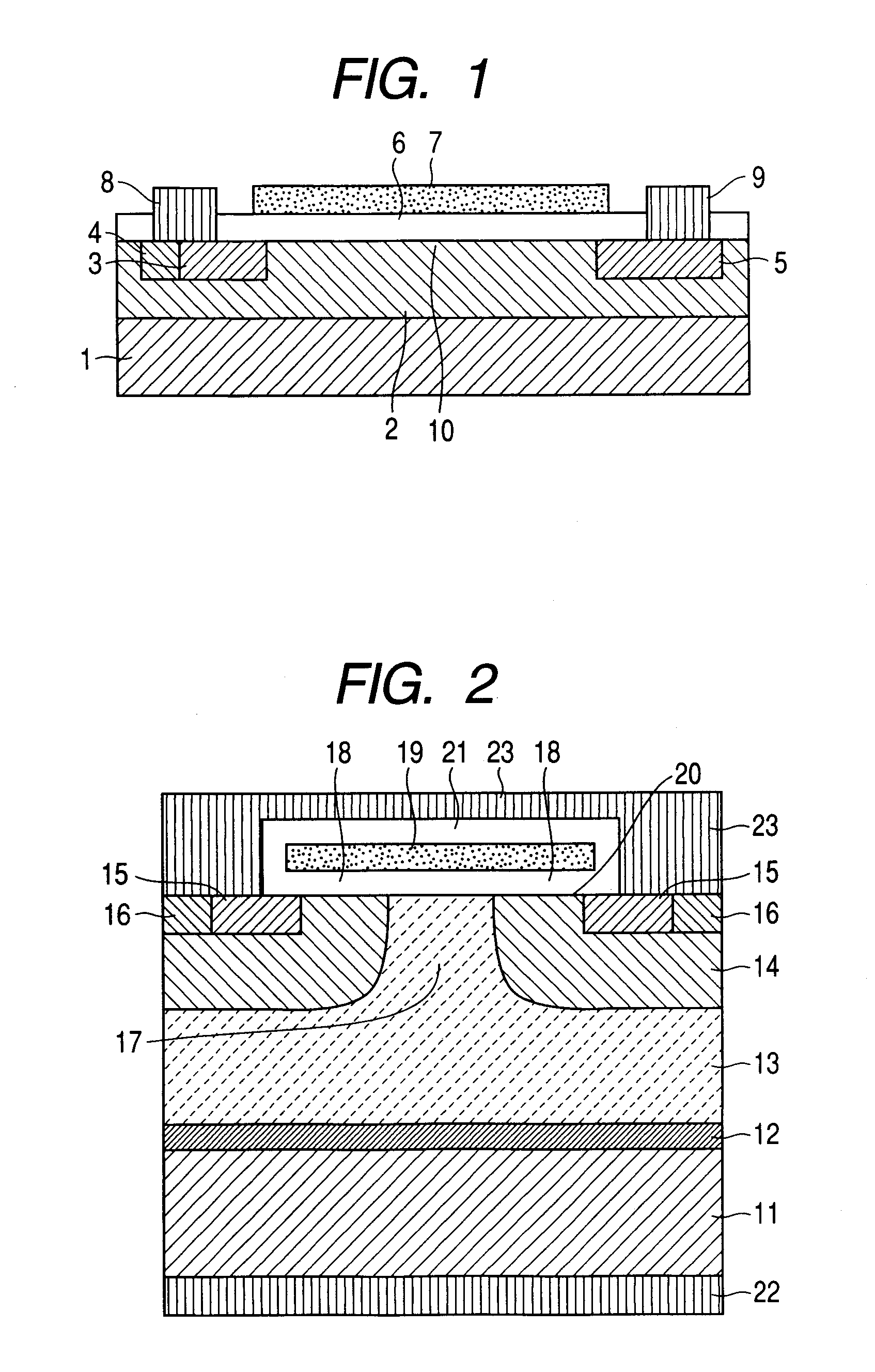
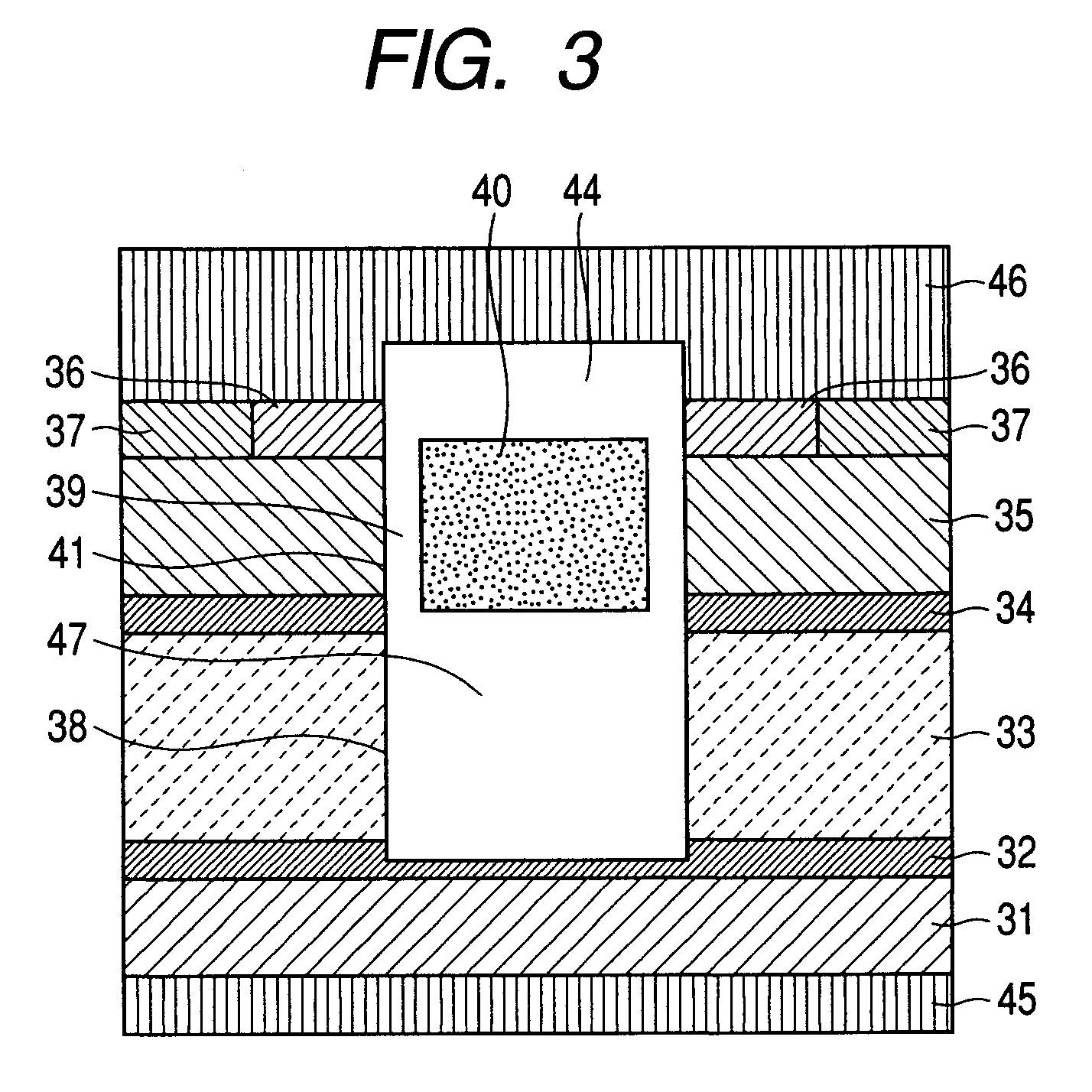
[0046]In Example 1, the manufacturing method of an n-type SiC-MOS capacitor according to the invention will be explained. Change in conduction type allows a p-type SiC-MOS capacitor to be manufactured in the same way as that in Example 1 explained below. Furthermore, by forming parts such as a drain, a source electrode and a gate electrode with a publicly known method, a device such as an n-channel or a p-channel MOSFET can be easily manufactured.

[0047]First, an alumina boat is prepared. Upstream from the boat, a SiC dummy substrate (which is not necessarily a single crystal) is disposed on which a 5 mm thick SiO2 has been deposited. The width of the dummy substrate sample to a gas flow is taken as at least wider than the width (50.8 mm in diameter) of a later described SiC substrate sample to be originally processed, 55 mm square, for example. Downstream from the boat, the SiC substrate sample is disposed for manufacturing the n-type SiC-MOS capacitor according to the inve...

Example

Example 2

[0058]In Example 2, a manufacturing method of an n-type SiC-MOS capacitor according to the invention will be also explained. As in the Example 1, a modification in the conductivity type of a SiC substrate of course allows a p-type MOS capacitor and n-channel or p-channel MOSFET to be formed. In the following, explanations will be made with particular emphasis on the difference from Example 1.

[0059]In Example 2, a double tube of silica glass is used as a heat treatment system. The system has a structure in which cooling water is made to flow between the outer tube and the inner tube of the double tube. A SiC substrate sample with the SiO2 according to the invention formed thereon and a dummy sample are mounted on a high purity graphite susceptor coated with polycrystalline SiC. The susceptor is set on a susceptor holder of silica glass with a thick felt of high purity porous graphite put between so that the susceptor does not make direct contact with the double tube of silic...

Example

Example 3

[0063]In Example 3, the manufacturing method of an n-type SiC-MOS capacitor according to the invention will be explained. As in Examples 1 and 2, a p-type MOS capacitor and n-channel or p-channel MOSFET can be formed. For Example 3, explanations will be made with particular emphasis on the difference from Examples 1 and 2.

[0064]The heat treatment system used in Example 3 is a system in which a hollowed heat insulator of high purity graphite is placed in a reaction tube of silica glass of a SiC epitaxial growth system and a high purity graphite susceptor coated with polycrystalline SiC is set inside the insulator to be provided as the heat treatment system for the SiO2 according to the invention. The graphite susceptor is horizontally grooved. Along the groove, a polycrystalline SiC substrate is placed. On the polycrystalline SiC substrate, a SiC substrate sample according to the invention and a dummy substrate are mounted (the dummy substrate is mounted upstream). The graph...


PUM


Abstract

A method of manufacturing a device on a silicon carbide substrate is disclosed. The device includes an oxide layer which has silicon oxide as a main component on the silicon carbide semiconductor substrate. The method includes depositing and oxide layer on a surface of the silicon carbide semiconductor substrate; raising a temperature of the oxide layer in a non-oxidizing atmosphere to a temperature bringing the oxide layer into a liquefied state; and then rapidly cooling the oxide layer down to a temperature equal to or less than 1140° C. to form the oxide layer including silicon oxide as a main component. The silicon carbide semiconductor device has improved channel mobility to lower on-resistance by decreasing an interface state density at an interface between the oxide insulator film that has silicon oxide as its main component and the silicon carbide semiconductor substrate.

Description

CROSS REFERENCE TO RELATED APPLICATIONS[0001]This application claims priority from application Serial No. JP 2006-114793, filed on Apr. 18, 2006, the contents of which are incorporated herein in their entirety.BACKGROUND OF THE INVENTION[0002]A. Field of the Invention[0003]The present invention relates to a silicon carbide semiconductor device formed as a device such as a MOSFET (insulated gate metal-oxide-semiconductor field effect transistor), an IGBT (insulated gate bipolar transistor), a bipolar transistor or a diode by using a silicon carbide semiconductor substrate, and a manufacturing method of the device.[0004]B. Description of the Related Art[0005]It is reported that a high breakdown voltage power device fabricated by using a silicon carbide (SiC) semiconductor substrate has a possibility of considerably lowering on-resistance of the device. In recent years, low on-resistance less than 10 mΩcm2 has been obtained in a MOSFET of SiC of 1.2 to 1.7 kV class. This is lower than ...

Claims


Application Information

Patent Timeline
IPC IPC(8): H01L21/31
CPCH01L21/049H01L21/3105H01L29/0878H01L29/1608H01L29/7813H01L29/6606H01L29/66068H01L29/7802H01L29/42368
Inventor NAKAMURA, SHUN-ICHIYONEZAWA, YOSHIYUKI
Owner FUJI ELECTRIC HLDG CO LTD
Why Eureka
Try Eureka