Multilayer circuit board and method for manufacturing the same

a multi-layer circuit board and manufacturing method technology, applied in the direction of sustainable manufacturing/processing, final product manufacturing, etching metal masks, etc., can solve the problems of long treatment time, difficult to form via-hole conductors between intended layers in the manufacture of multi-layer circuit boards, and high chemical content in chemical plating, etc., to achieve high melting point, high electrical conductivity, and high heat resistance

Active Publication Date: 2013-11-14
MURATA MFG CO LTD
View PDF2 Cites 30 Cited by
  • Summary
  • Abstract
  • Description
  • Claims
  • Application Information

AI Technical Summary

Benefits of technology

[0030]The present invention can provide a multilayer circuit board including a via-hole conductor having higher heat resistance than before, and a method for manufacturing the multilayer circuit board. The multilayer circuit board has high electrical conductivity and connection reliability.
[0031]In accordance with a method for manufacturing a multilayer circuit board according to the present invention, use of an electroconductive paste having the composition described above simultaneously allows the low-melting-point component (for example, Sn having a melting point of 232° C.) in the electroconductive paste within the via-hole to be entirely converted into a high-melting-point intermetallic compound t...

Problems solved by technology

However, such a method disadvantageously requires an expensive chemical in chemical plating and a long treatment time.
Furthermore, it is difficult to form a via-hole conductor between intended layers in the manufacture of a multilayer circuit board.
Thus, the density of the conductive wiring layers cannot be sufficiently increased.
However, because of a low diffusion velocity of Sn in a reaction between Ag or Cu and Sn, complete alloying of Sn takes a long time.
Thus, a short heat treatment results in the presence of unreacted Sn (low-melting-point metal) in a via-hole conductor and consequently low heat resistance of the via-hole conductor.
However, in a reaction between a hig...

Method used


Image

  • Multilayer circuit board and method for manufacturing the same
  • Multilayer circuit board and method for manufacturing the same
  • Multilayer circuit board and method for manufacturing the same

Examples


embodiment 1

[0118]A multilayer circuit board according to the present embodiment includes a via-hole conductor for electrically connecting conductive wiring layers in a resin layer.

[0119]A method for manufacturing a multilayer circuit board according to an embodiment of the present invention will be described below with reference to FIGS. 2 and 3.

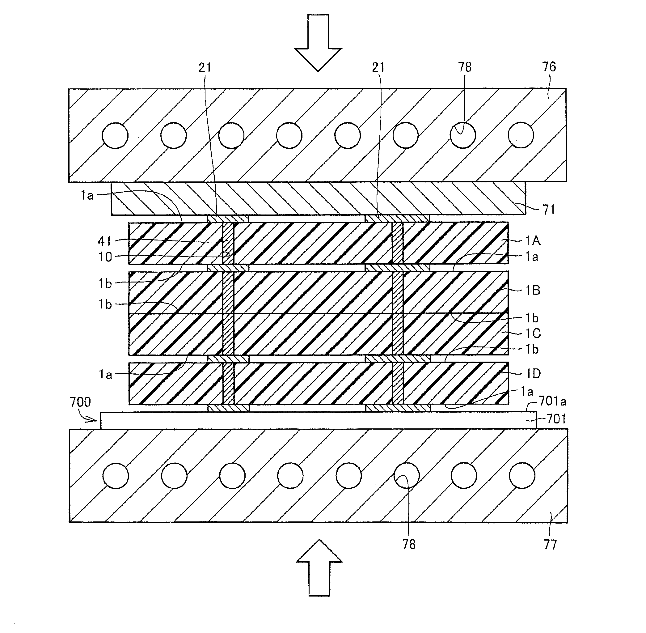
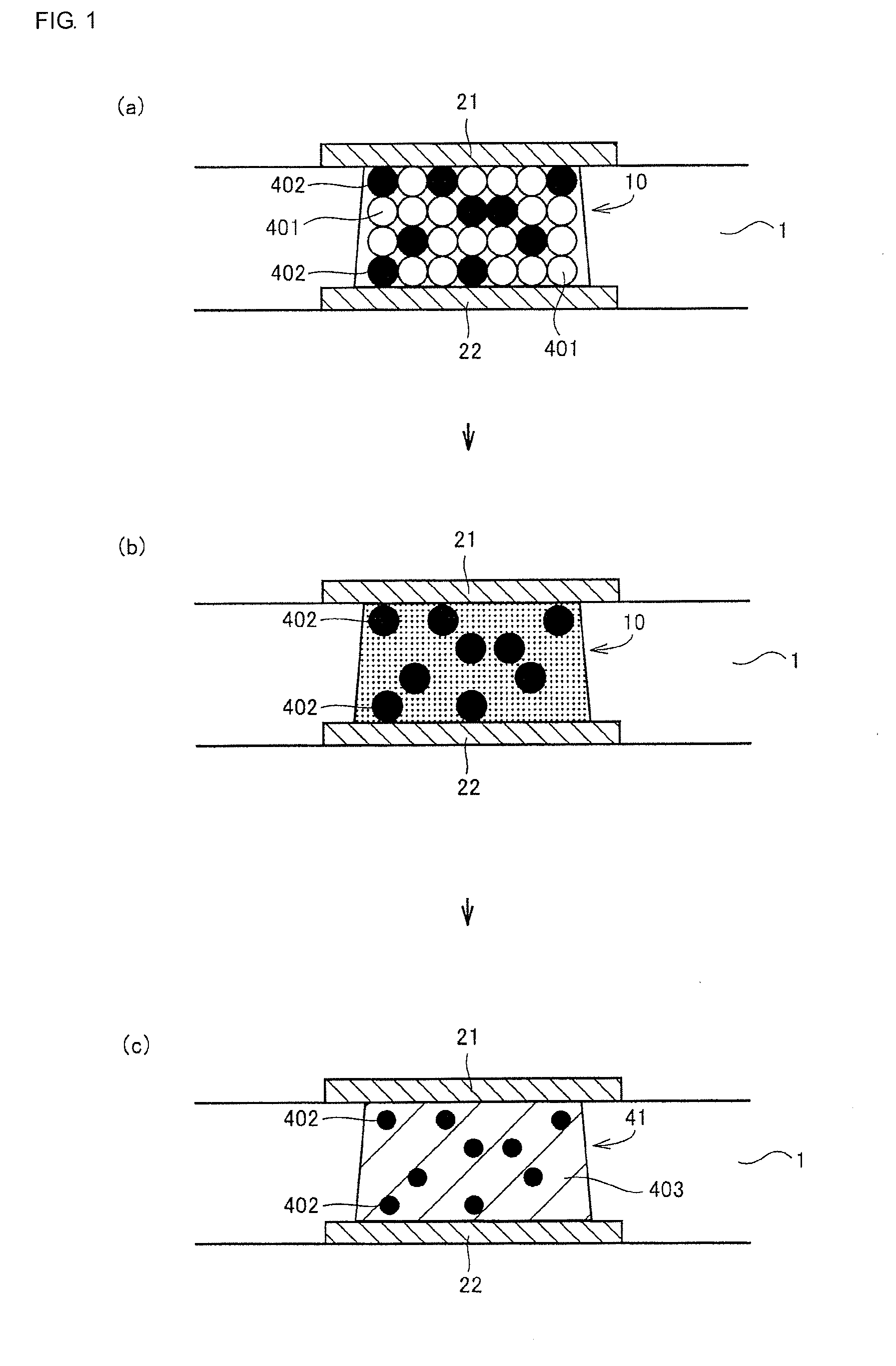
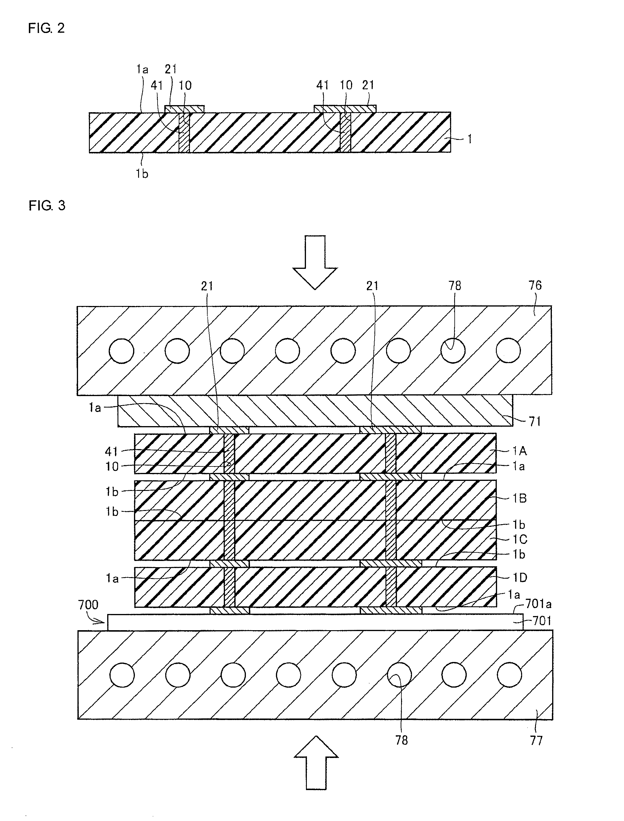
[0120]Referring to FIG. 2, a via-hole 10 is formed from the back side (surface 1b) of a resin sheet to a conductive wiring layer 21. The via-hole 10 is formed through laser processing using a carbon dioxide laser or the like at each location at which an inner via (via-hole conductor) is to be formed. After boring a hole in the resin sheet, smears of resin residues are removed.

[0121]The via-hole 10 is then filled with an electroconductive paste, for example, by screen printing to form a via-hole conductor 41. The electroconductive paste produces an intermetallic compound having a melting point of 300° C. or more by a reaction between the first metal and...

embodiment 2-1

[0135]A multilayer circuit board according to the present embodiment includes resin layers, which include a via-hole conductor for electrically connecting conductive wiring layers to each other. The multilayer circuit board includes an electronic component having an external electrode.

[0136]The via-hole conductor containing the intermetallic compound described above is more rigid and less flexible than copper for use in electrodes. Thus, the via-hole conductor can protect the electronic component from bending stress.

[0137]When the intermetallic compound is produced by a reaction between Sn and Cu—Ni, the diffusion velocity of Sn and Cu—Ni is 10 times or more higher than the diffusion velocity of a Sn and Ag or Sn and Cu metal system. The resulting via-hole conductor therefore generally has fine pores (voids). The pores act as cushions against external impacts or loads and reduce impacts or loads on the electronic component. Thus, a low-profile multilayer circuit board that includes ...

embodiment 2-2

[0147]A multilayer circuit board according to the present embodiment will be described below with reference to FIG. 6. The processes illustrated in FIGS. 5(a) to 5(g) in the present embodiment are the same as in Embodiment 2-1 and will not be further described.

[0148]An electronic component 5 is appropriately placed while a plurality of resin layers are stacked. The electronic component 5 is finally disposed in the cavity 11 (FIG. 6(h)). In the present embodiment, a via-hole 101 is disposed at a location at which a protective via-hole conductor 411 not connected to a conductive wiring layer 21 is to be formed. The via-hole 101 is filled with an electroconductive paste 401. The electroconductive paste 401 is composed of the same material as the via-hole conductor 40.

[0149]The resin layers are stacked such that the surfaces of adjacent resin layers 1 on which the conductive wiring layer 21 is disposed do not face each other. The electronic component 5 includes an external electrode 51 ...


PUM

PropertyMeasurementUnit
Fractionaaaaaaaaaa
Percent by massaaaaaaaaaa

Abstract

The present invention provides a multilayer circuit board that includes a plurality of resin layers, conductive wiring layers, and via-hole conductors. Each of the resin layers includes a resin sheet containing a resin and a conductive wiring layer disposed on at least one surface of the resin sheet. The via-hole conductors contain an intermetallic compound having a melting point of 300° C. or more produced by a reaction between a first metal composed of Sn or an alloy containing 70% by weight or more Sn and a second metal composed of a Cu—Ni alloy or a Cu—Mn alloy. The second metal has a higher melting point than the first metal.

Description

CROSS REFERENCE TO RELATED APPLICATIONS[0001]The present application is a continuation of PCT / JP2012 / 053542 filed Feb. 15, 2012, which claims priority to Japanese Patent Application No. 2011-029754, filed Feb. 15, 2011, Japanese Patent Application No. 2011-033490, filed Feb. 18, 2011, Japanese Patent Application No. 2011-037305, filed Feb. 23, 2011, Japanese Patent Application No. 2011-043972, filed Mar. 1, 2011, Japanese Patent Application No. 2011-045114, filed Mar. 2, 2011, Japanese Patent Application No. 2011-045409, filed Mar. 2, 2011, and Japanese Patent Application No. 2011-045528, filed Mar. 2, 2011, the entire contents of each of which are incorporated herein by reference.FIELD OF THE INVENTION[0002]The present invention relates to a multilayer circuit board manufactured by stacking a plurality of resin layers, each of which includes a resin sheet and a conductive wiring layer disposed on the resin sheet.BACKGROUND OF THE INVENTION[0003]In recent years, resin multilayer cir...

Claims


Application Information

Patent Timeline
IPC IPC(8): H05K1/09H05K3/42H05K1/11
CPCH05K1/092H05K1/115H05K3/429H05K1/0271H05K1/185H05K3/4038H05K3/4617H05K2201/0305H05K2201/09527H05K2201/09781H05K2201/10636H05K2203/063H05K3/0052H05K3/4069H05K3/4632H05K2201/096H05K2203/0554H01L2224/16225H01L2924/1533Y10T29/49165Y02P70/50
Inventor CHISAKA, SHUNSUKESOMADA, HIROSHINAKANO, KOSUKEKATO, NOBORU
Owner MURATA MFG CO LTD
Why Eureka
Try Eureka