

Method and device for using substrate geometry to determine optimum substrate analysis sampling
- Summary
- Abstract
- Description
- Claims
- Application Information
AI Technical Summary
Benefits of technology
Problems solved by technology
Method used
Image

Examples
Embodiment Construction
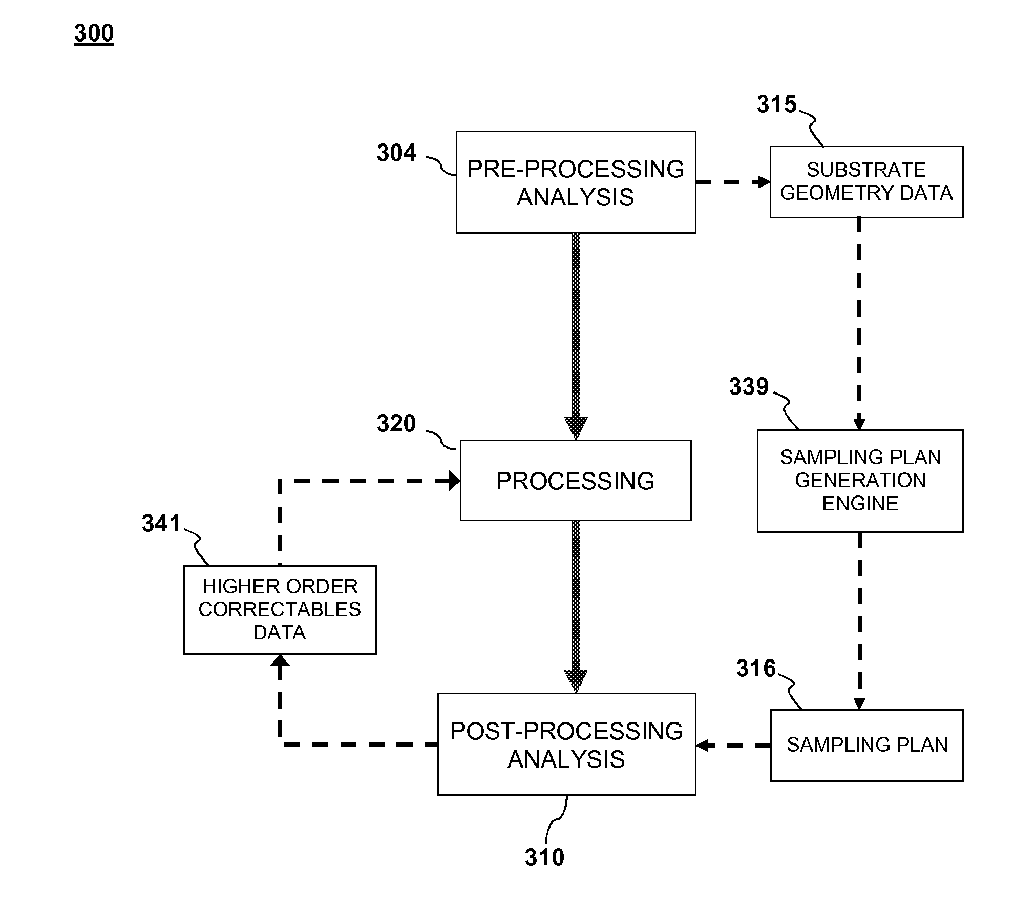
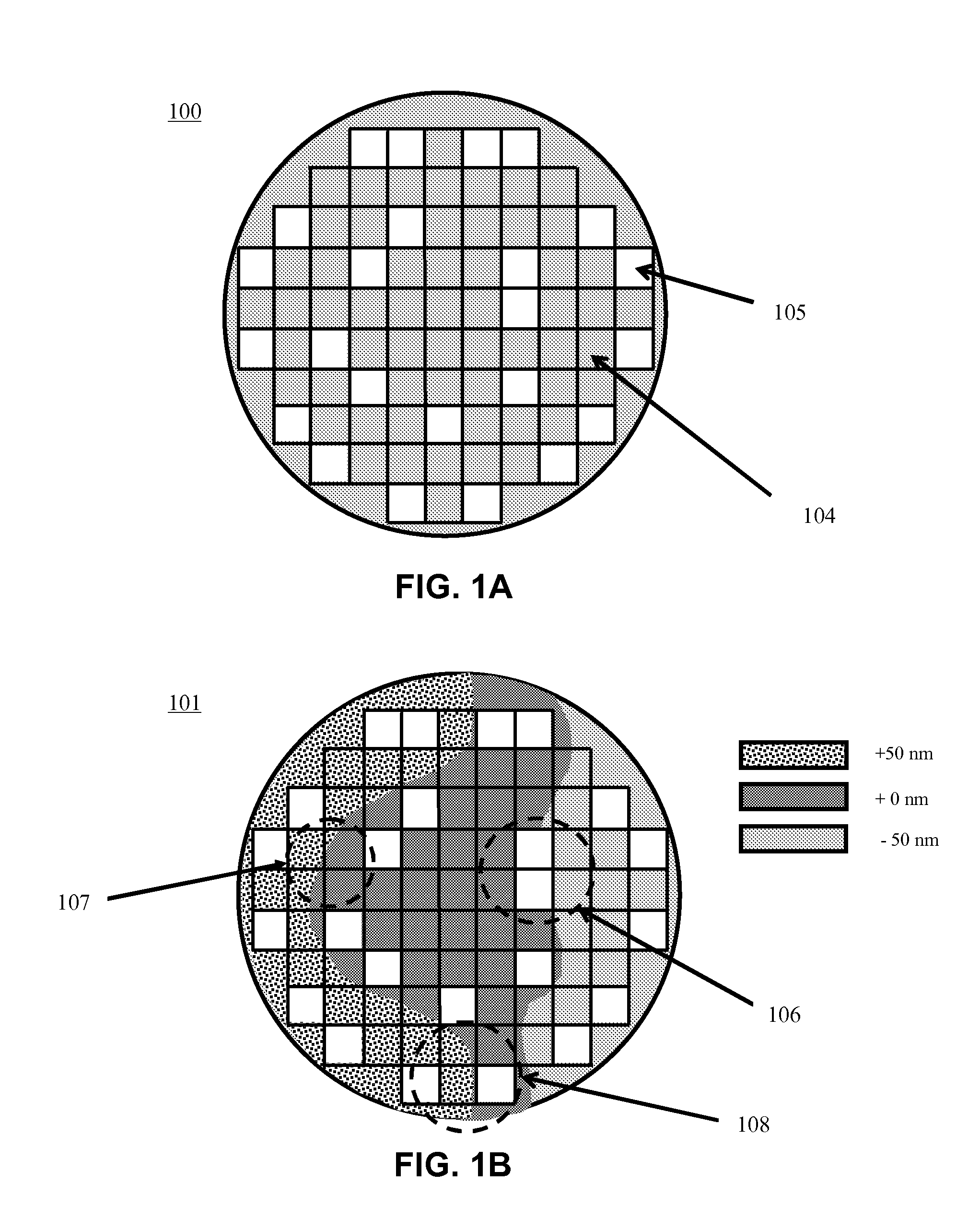
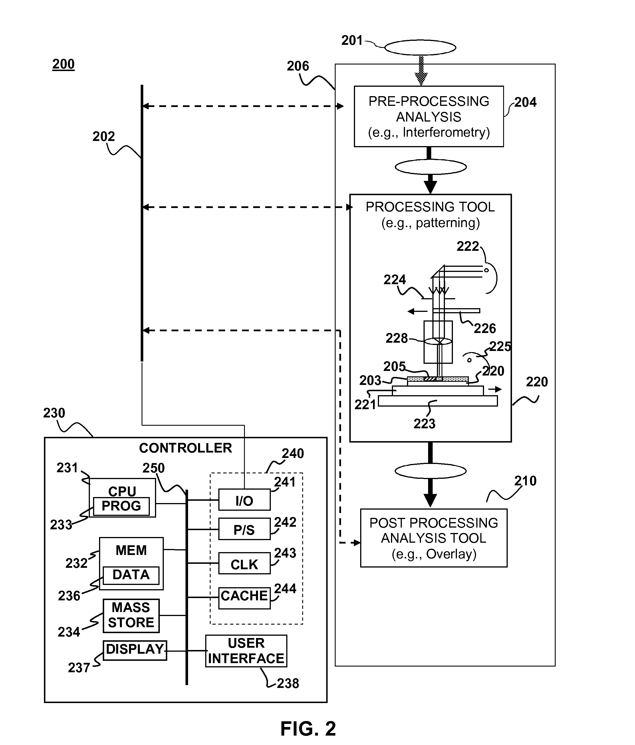
[0019]Although the following detailed description contains many specific details for the purposes of illustration, anyone of ordinary skill in the art will appreciate that many variations and alterations to the following details are within the scope of the invention. Accordingly, the exemplary embodiments of the invention described below are set forth without any loss of generality to, and without imposing limitations upon, the claimed invention.
[0020]In the following description, reference is made to the accompanying drawings, which form a part hereof, and in which is shown by way of illustration specific embodiments in which embodiments of the invention may be practiced. In this regard, directional terminology, such as “top,”“bottom,”“front,”“back,”“leading,”“trailing,” etc., is sometimes used with reference to the orientation of the figure(s) being described. Because components of embodiments of the present invention can be positioned in a number of different orientations, the di...
PUM
 Abstract
Description
Claims
Application Information