Phase-combining circuit and timing signal generator circuit for carrying out a high-speed signal transmission

a timing signal and generator circuit technology, applied in pulse manipulation, pulse technique, instruments, etc., can solve the problems of increasing the size of the chip, interrupting the improvement in the performance of the computer, and no longer being able to improve the performance of the system, etc., and achieve the effect of simple structur

Inactive Publication Date: 2013-11-28
FUJITSU LTD
View PDF3 Cites 82 Cited by
  • Summary
  • Abstract
  • Description
  • Claims
  • Application Information

AI Technical Summary

Benefits of technology

The present invention provides a high-precision timing signal generator circuit that uses a small number of input phases. This circuit does not require a phase selector circuit that can cause phase errors and jitter. The correction control circuit can correct the second digital control code to minimize errors between the output clock and a desired reference phase. The first control code can be defined by interpolating between the correction points. These technical effects improve the accuracy and stability of the timing signal generator circuit.

Problems solved by technology

Along with the improvement in the performance of semiconductor memories and processors, it has now come to a stage where it is no longer possible to improve the performance of systems without improving the signal transmission speed between parts and between elements.
This speed gap has come to interrupt the improvement in the performance of computers in recent years.
Along with an increase in the size of chips, this gap in the signal transmission speed between elements within one chip and between circuit blocks has been a large factor that limits the performance of chips, not only the signal transmission between chips (between LSI chips).
However, in the case of using a large number of interpolators in a multi-channel signal transmission, it is difficult to distribute a multi-phase clock (for example, a clock of twelve phases) by keeping a mutual positional relationship within the chip.
Further, it is also difficult to realize a circuit of a small phase error that selects two specific signals (phases) from among a large number of input signals having different phases.
Because of this influence, there occurs a problem that a timing error (jitter) becomes larger at a boundary where the phase is changed over due to a residual coupling from the input phase to the output, even if the input signal has a zero nominal weight in its phase.
This jitter can become a fatal problem for the timing signal generator circuit for high-speed signal transmission that always requires a correct timing signal.

Method used


Image

  • Phase-combining circuit and timing signal generator circuit for carrying out a high-speed signal transmission
  • Phase-combining circuit and timing signal generator circuit for carrying out a high-speed signal transmission
  • Phase-combining circuit and timing signal generator circuit for carrying out a high-speed signal transmission

Examples


first embodiment

[0127]As shown in FIG. 5, the timing signal generator circuit of the first embodiment is constructed of the four-phase clock generator circuit that receives a reference clock elk synchronous with a clock supplied from the outside of the chip via the PLL circuit 2, the control signal generator circuit 4, and the phase-combining circuit 5.

[0128]The output signal (timing signal) CK of the phase-combining circuit 5 is supplied to the receiver 3, for example, and the transmitted data is received. The receiver 3 compares the phase of the data clock supplied from the outside with the phase of the internal clock (the output of the timing signal generator circuit) CK. The receiver then feeds back a signal according to a result of the phase comparison to the phase-combining circuit 5 via the control signal generator circuit 4. As described above, the receiver 3 (signal reception circuit) is only one example, and the timing signal generator circuit of the present embodiment can also be applied...

second embodiment

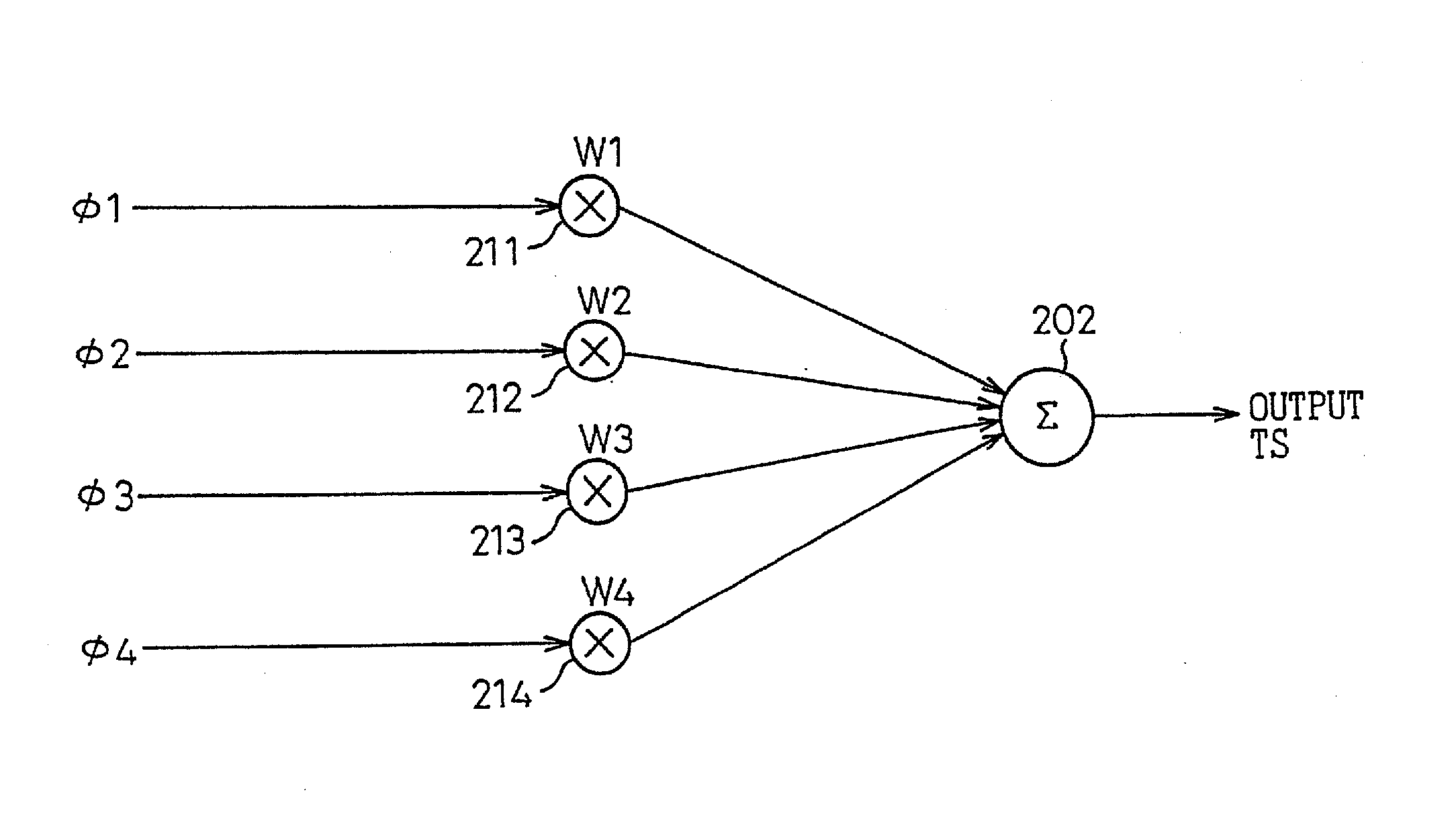
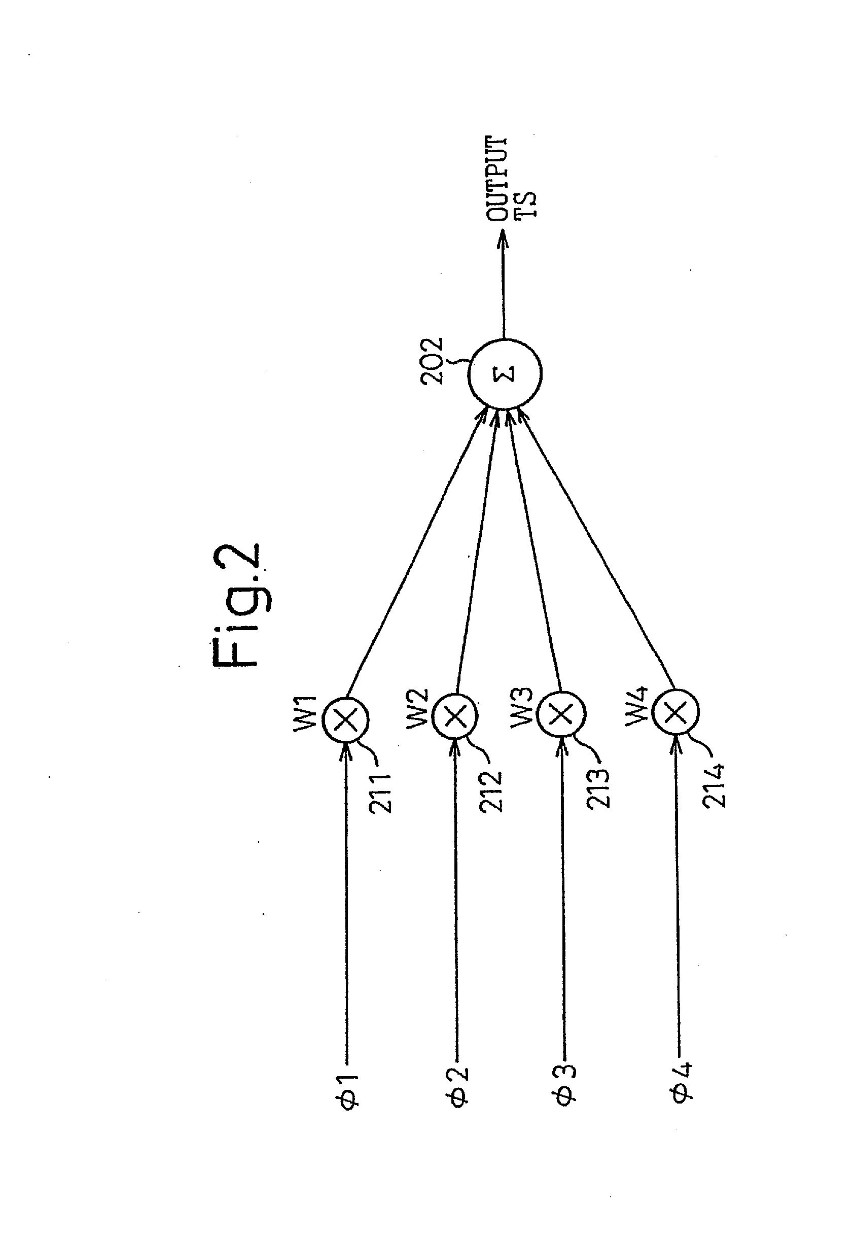
[0167]FIG. 20 is a block circuit diagram showing one example of a phase-combining circuit as the timing signal generator circuit relating to the present invention. In FIG. 20, a reference number 530 denotes a D / A converter, 541 to 544 denote weight processing circuits, 550 denotes a pre-driver, and 560 denotes a mixer and output buffer.

[0168]As shown in FIG. 20, the phase-combining circuit 5 is constructed of the D / A converter 530, the weight processing circuits 541 to 544, the pre-driver 550, the mixer and output buffer 560, and inverters 571 and 572.

[0169]The D / A converter 530 is applied with inputs of a reference current Ir and a plurality of control codes such as, for example, complementary 18-bit control codes CD0, / CD0 to CD8 and / CD8, and CD10, / CD10 to CD18 and / CD18. The D / A converter 530 then outputs four weights (currents) W1 to W4 corresponding to these control codes. A reference symbol TES denotes a testing signal that is used for testing a circuit. The weight processin...

fourth embodiment

[0197]FIG. 32 is a circuit diagram showing one example of a phase-combining circuit as the timing signal generator circuit relating to the present invention.

[0198]As shown in FIG. 32, a phase-combining circuit 7100 of the fourth embodiment uses two input phases fl and a, and is constructed of p-MOS transistors 7101 to 7104, n-MOS transistors 7105 to 7116, and a comparator (differential amplifier) 7117. The transistors 7105, 7106, 7108, 7109, 7111, 7112, 7114 and 7115 constitute pairs of differential amplifiers respectively. These transistors give the weight W1 to the gate of the transistor 7107, give the weight W2 to the gate of the transistor 7116, and give a fixed weight W0 to the gates of the transistors 7110 and 7113 respectively.

[0199]More specifically, according to the phase-combining circuit 7100 of the fourth embodiment, the four phases φ1 to φ4: φ1, / φ1 to φ4, / φ4) are not input like the phase-combining circuit 5 shown in FIG. 11, but the two phases (φ1, φ2: φ1, / φ1, φ2, / φ...


PUM


Abstract

A phase-combining circuit for combining cyclic timing waveforms that have been phase-controlled by control signals based on three or more input signals of different phases, has a weight signal generating circuit and a weighting circuit. The weight signal generating circuit generates weights according to the control signals, and the weighting circuit gives the weights to the respective input signals, with a positive or negative polarity for each one signal.

Description

CROSS-REFERENCE TO RELATED APPLICATION[0001]This application is a Divisional of prior application Ser. No. 13 / 064,429 filed on Mar. 24, 2011, which is a Divisional of prior application Ser. No. 12 / 320,698, now abandoned, filed on Feb. 2, 2009, which is a Divisional of prior application Ser. No. 09 / 714,650, now abandoned, filed on Nov. 17, 2000, the entire contents of each of which being incorporated herein by reference. This application is based upon and claims the benefit of priority from the prior Japanese Patent Application No. 11-336328, filed on Nov. 26, 1999, Japanese Patent Application No. 2000-080792, filed on Mar. 22, 2000, and Japanese Patent Application No. 2000-312181, filed on Oct. 12, 2000, the entire contents of each of which are incorporated herein by reference.FIELD OF THE INVENTION[0002]The present invention relates to a phase-combining circuit and a timing signal generator circuit, and more particularly, to a phase-combining circuit and a timing signal generator c...

Claims


Application Information

Patent Timeline
Patent Type & Authority Applications(United States)
IPC IPC(8): G06G7/12H03K7/08H03K5/00H03K5/13H03K5/151H03L7/07H03L7/081H03L7/089H04L7/033
CPCG06G7/12H03K5/13H03K5/133H03K5/151H03K2005/00026H03K2005/0013H03K2005/00208H03L7/07H03L7/0816H03L7/0891H04L7/033H03K7/08
Inventor TAMURA, HIROTAKAKIBUNE, MASAYA
Owner FUJITSU LTD
Why Eureka
Try Eureka