Where the application is very
cost sensitive it may be too expensive to use such wettable polymers, and for many inexpensive plastics an
inert gas treatment has been found not to be effective in promoting adequate adhesion of the hard
coating.
This technique works quite well at substrate temperatures less than or about 100° C. but it generates substantial heat and produces films that are often not as amorphous and effective as barriers.
In some applications where the plastic or
polymer substrate is thick or cannot be cooled effectively
sputtering may not be acceptable due to heating of the substrate.
Plasma enhanced CVD has been used very predominantly in applications where the limiting temperature for the substrate is above about 200° C., but has not been capable of providing commercially competitive rates of deposition of high quality dielectrics at substrate temperatures under 100° C. The approach of Savas et al (US 20110006040, 20110005682, and 20110005681) offers promise that
plasma enhanced CVD can provide dense homogeneous barrier films at such temperatures and at reasonable cost.
But there are also substantial technological challenges to be solved before
OLED displays larger than a
square decimeter—such as useful for tablet or
laptop displays—can be manufactured with high yield.
In particular, the very thin, low work-function metals used for the
electron emitting layer in an OLED device are
highly sensitive to damage by oxidation.
Currently this can only be done in
mass production using a top covering of glass which is 100 or more microns thick.
High-vacuum chambers with such a high degree of vacuum integrity are not uncommon, but require careful design, are expensive to make and are not generally
mass-produced.
This is an expensive technique ($50 / m2 to $100 / m2) and only suitable for relatively small and rigid displays, such as on smart phones or tablets.
It also suffers from difficulty relating to stresses when front and back surfaces are not maintained at precisely the same temperature.
The consequent leaking of
atmosphere into the sensitive material
layers destroys the device and makes a “
black spot” on the screen or lighting panel.
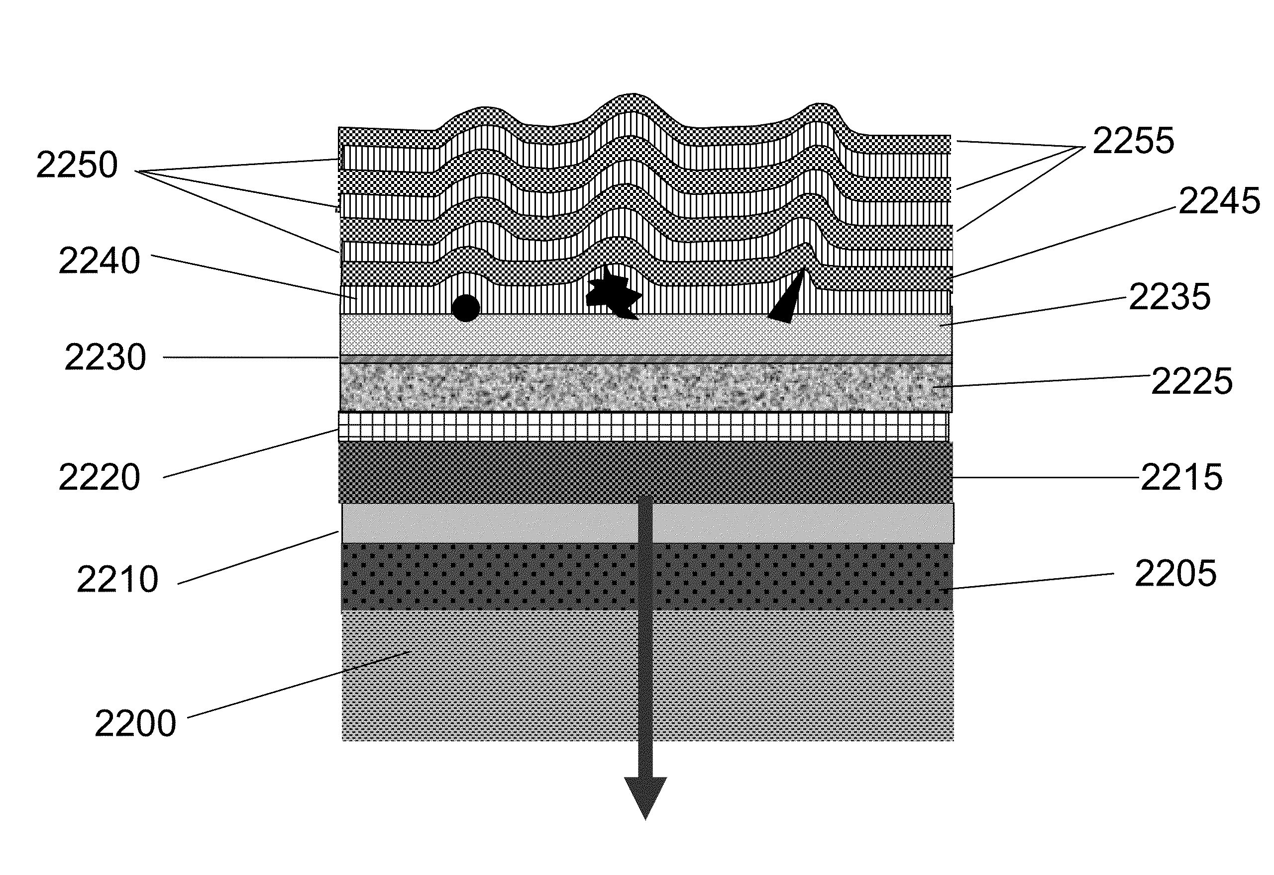
However, under
mass production conditions deposited films will have localized areas where the film does not have adequate
barrier function.
Such defects result from undesirable film morphology or insufficient
film density that leads to localized areas that have higher transmission of
oxygen and
water vapor.
Such defects may be caused by particles on the starting substrate, areas on the substrate with higher
nucleation energy, particles generated during the deposition, overhanging or re-entrant surface
topography and film cracks due to poor adhesion or stress.
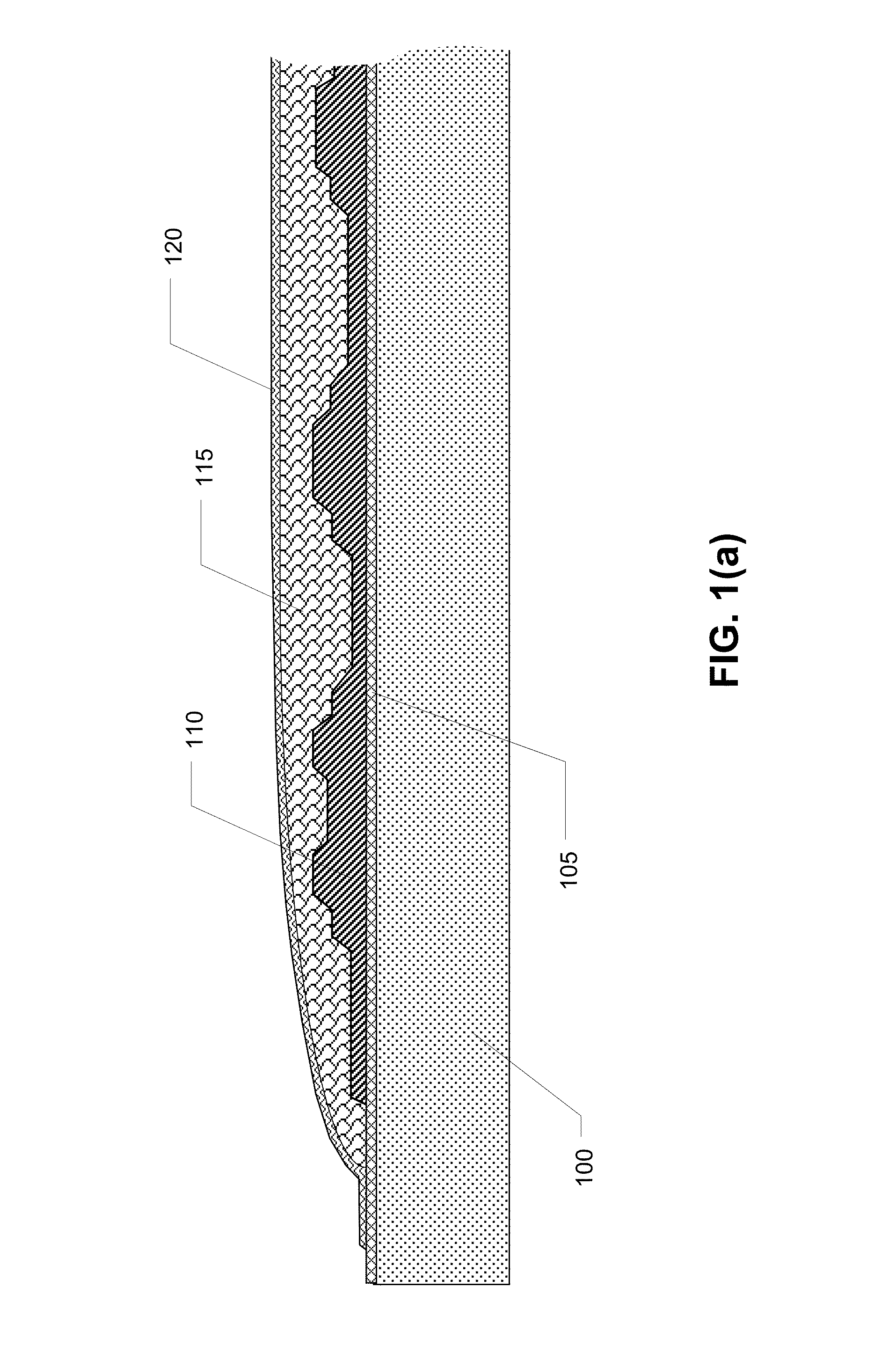
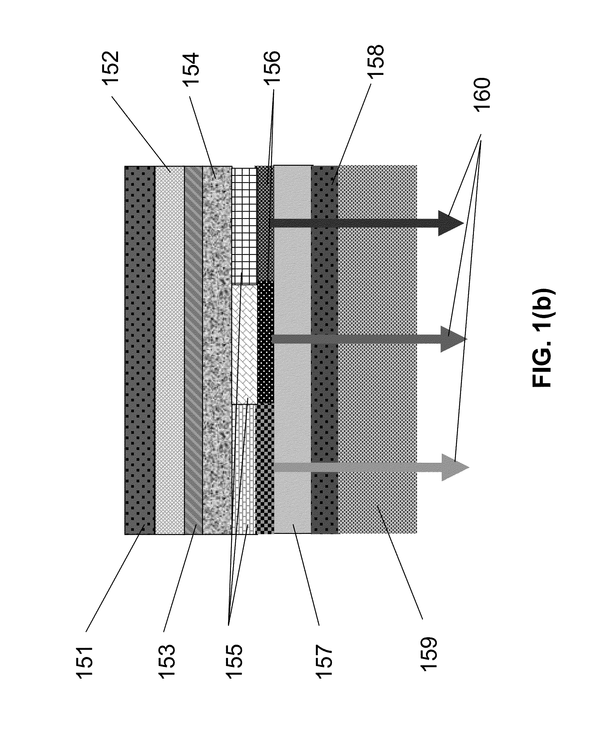
Another challenge to the application of thin barrier films to polymeric substrates in particular (and other surfaces in general) is the difficulty of obtaining adequate adhesion of the coating to the underlying material.
Additional adhesion enhancement methods include deposition of thin metallic ‘primer’
layers using
evaporation or
sputtering, but these approaches can compromise the
optical quality and operation of the display.
Some services are able to measure levels about an
order of magnitude lower, but are not able to distinguish between
moisture leakage due to localized defects or due to bulk permeability.
While very thin (<30 nm) inorganic films such as
silicon dioxide and
silicon nitride accommodate substantial expansion without
cracking, thicker films do crack.
There are currently no known deposition processes that can produce said coatings within the cost limits.
The above techniques do not allow for a method to monitor defect levels in production directly, and in the case of final test may not catch the effect a long transmission path due to distributed defects in
multiple layer stacks.
The end result may be a display that works well initially, but may fail in a year of two, creating a negative
perception in the
market place.

