Conformally Encapsulated Multi-Electrode Arrays With Seamless Insulation

a technology of seamless insulation and encapsulation, applied in the field of multi-electrode arrays, can solve problems such as device failure, electrical shorts, trace metal corrosion, etc., and achieve the effects of reducing failure opportunities, enhancing adhesion, and improving adhesion

Active Publication Date: 2013-12-26
LAWRENCE LIVERMORE NAT SECURITY LLC
View PDF1 Cites 56 Cited by
  • Summary
  • Abstract
  • Description
  • Claims
  • Application Information

AI Technical Summary

Benefits of technology

[0013]While in the suspended state, the trace beams are encapsulated, either individually or together, with a single continuous layer, film, or coating of an electrically insulating material, such as for example ceramics, oxidized metals, dielectrics, polymers. In particular materials that may be vapor-deposited may be used, such as for example polyimides, parylene, polyurethanes, polycarbonates. Because the trace beam is encapsulated while suspended, the single insulating layer forms a seamless block of electrically insulating material that conforms to the shape of the trace beam structure, including any trace backings which provide suspension support. By encapsulating the conductive traces and electrodes of the array with a single coating of an insulator, multiple-layered polymers are eliminated, along with the associated delamination concerns at the polymer-polymer interfaces / seams and polymer-metal interfaces / seams when exposed to external fluids, thereby reducing opportunities for failure.
[0014]One advantage of this method of directly encapsulating the trace structure with a polymer or other insulating material is that the entire surface of the suspended structure can be treated with an adhesion promoting material to enhance adhesion between itself and the encapsulating material. This may involve either treating the surface of bare suspended metal traces, or treating a composite of trace metal and backing material that make up the suspended structure. Adhesion promoters may also be applied in between the trace metal and backing material that make up the suspended structure. For example, an adhesion promoter can be applied to the suspended traces that promotes covalent bonds with a polymer that is cured directly onto the metal. Or, an intermediate metallic layer can be deposited on the traces onto which the encapsulating material will adhere better. Adhesion-promoting materials include metals (e.g. titanium, titanium-nitride, chrome), dielectrics (e.g. silicon dioxide, silicon nitride) or organic and non-organic (e.g. organic and non-organic chemicals with the appropriate chemical groups to adhere the trace and electrode material to the trace backing and the encapsulation polymer) adhesion promoters. The adhesion-promoting layer may be deposited using vapor deposition, spin coating, atomic layer deposition, or oxidation (but not limited to these techniques).
[0015]The following are some examples of treatments that can improve adhesion between different layers: (1) the adhesion promoter A-174 silane may be vapor deposited onto the suspended structure to promote adhesion of parylene that is subsequently deposited as the encapsulating material; (2) the trace metal may consist of a stack of metals, with the outer (top and bottom) layers being a metal such as titanium onto which the encapsulating material will adhere better; (3) the liquid adhesion promoter, HD Microsystems VM-652, may be applied on top of the trace metal film to enhance adhesion of a polyimide layer that is subsequently spin-deposited to create a backing layer; (4) in the case of a backing structure that consists of a top and bottom layer of polyimide, the bottom polyimide layer may be treated with KOH followed by HCl in order to create a surface layer of polyamic acid. Then, this surface layer will cure (i.e. convert back to polyimide) together with the top layer of polyimide, improving adhesion between the two layers.

Problems solved by technology

However, such probes and devices typically require invasive surgeries for implantation, and also often require additional surgeries to remove and replace devices that have failed or otherwise require maintenance or servicing.
Penetration of bodily fluids at these compromised areas can result in trace metal corrosion, electrical shorts between interconnects, and ultimately device failure.
Therefore, maintaining adequate adhesion between adjacent layers of polymer and polymer-metal layers is a consistent concern using this approach, and one of the reasons thin-film microelectrode arrays have been unsuccessful for long term implantation.
However, these methods have largely failed by either not providing sufficient improvements in adhesion, or the polymer treatment parameters required for effective adhesion is detrimental to the metal thin films.

Method used


Image

  • Conformally Encapsulated Multi-Electrode Arrays With Seamless Insulation
  • Conformally Encapsulated Multi-Electrode Arrays With Seamless Insulation
  • Conformally Encapsulated Multi-Electrode Arrays With Seamless Insulation

Examples


Embodiment Construction

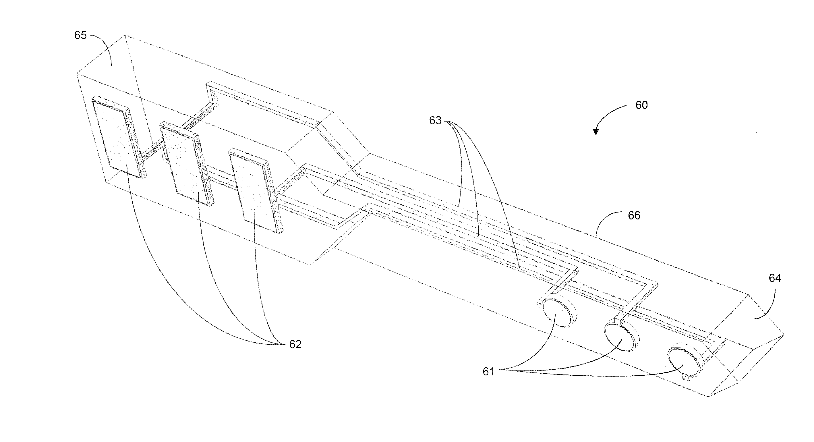
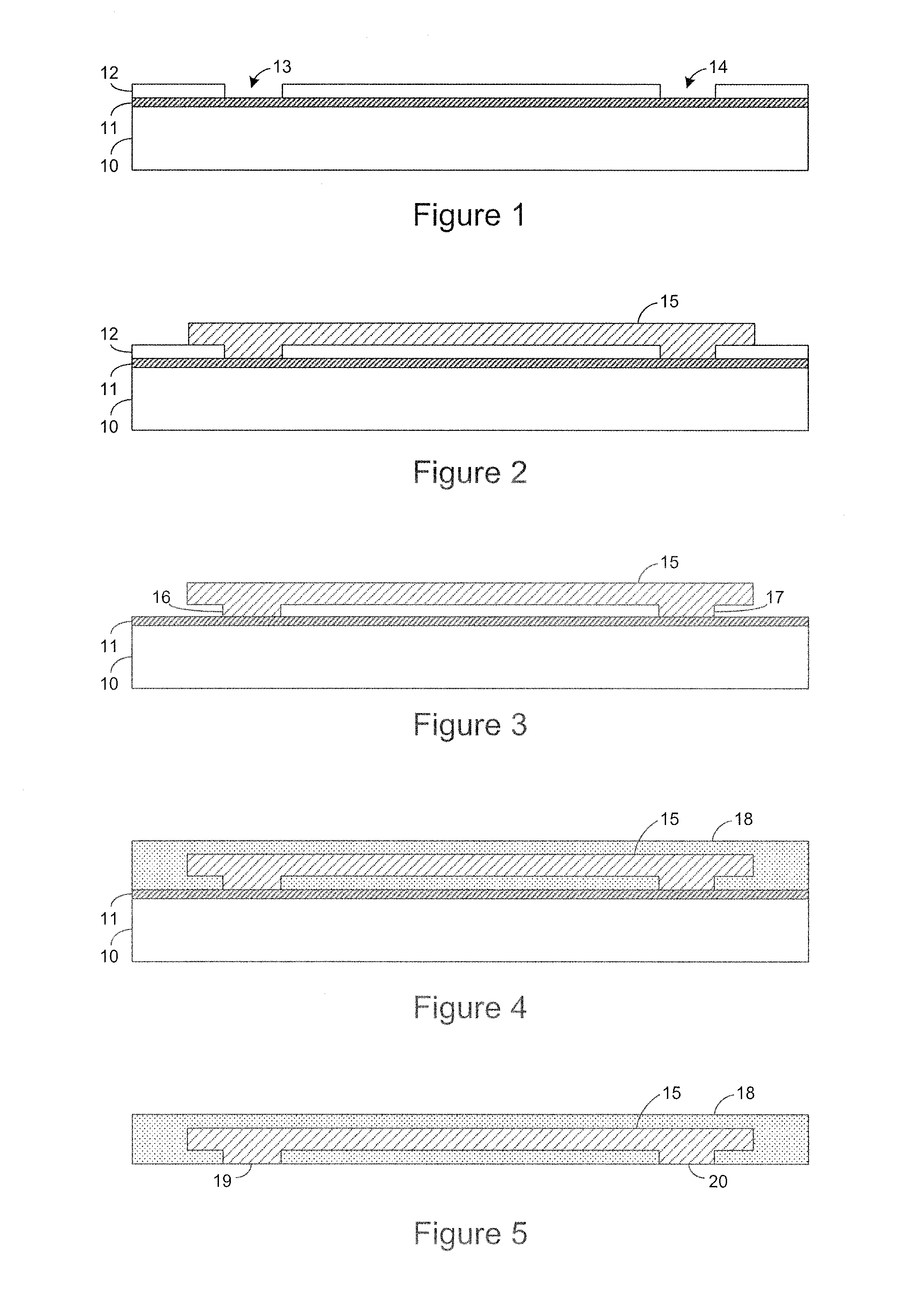
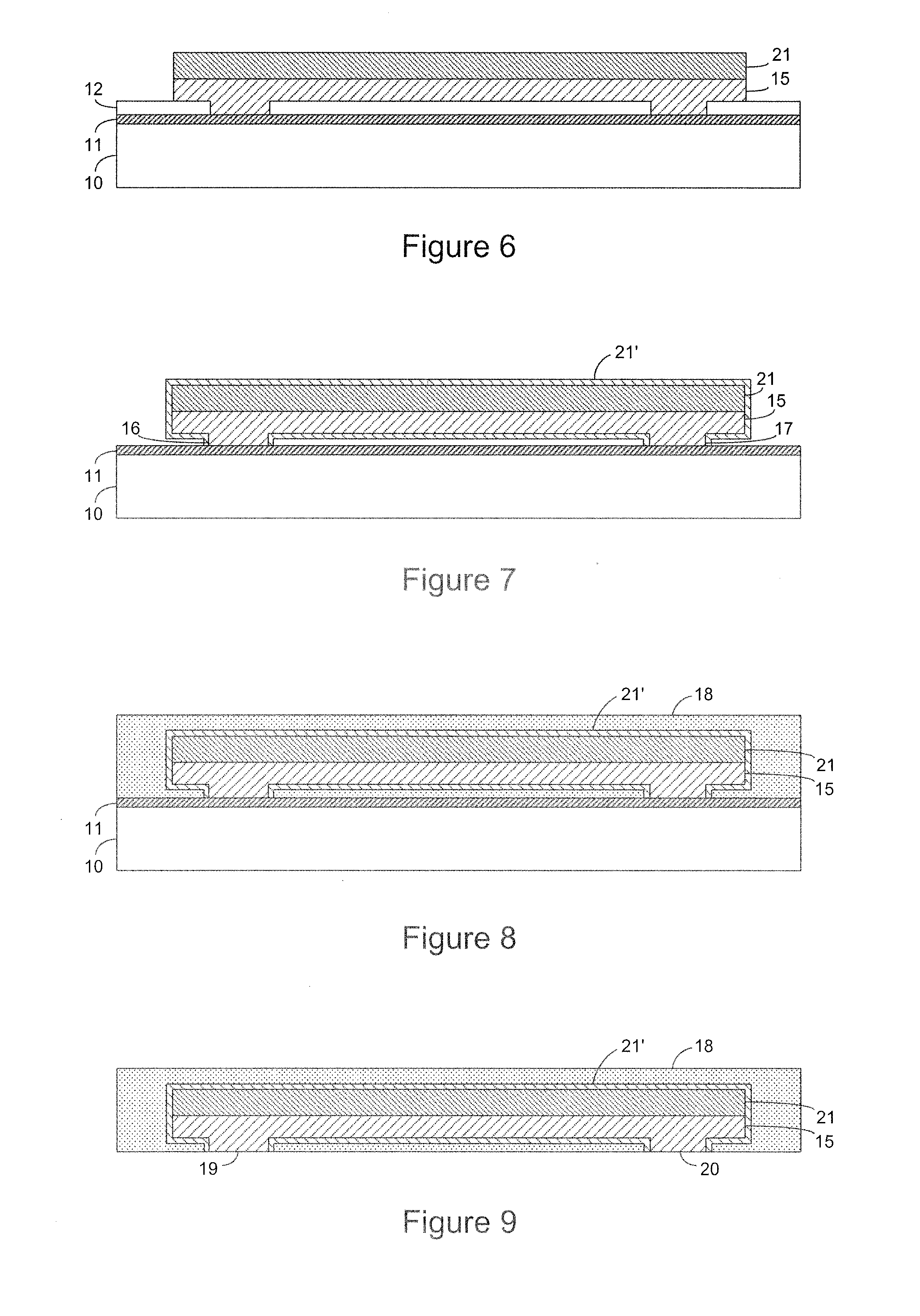
[0025]Turning now to the drawings, FIGS. 1-5 show a first example embodiment of the method of fabricating a conformally encapsulated electrode array of the present invention, and the electrode array formed thereby.

[0026]In particular, FIG. 1 shows a substrate having three layers, including a lower layer 10 which may be characterized as a handle wafer; a middle or embedded layer 11 which may be characterized as a release layer; and an upper layer 12 which may be characterized as a sacrificial layer. Via openings 13, 14 are also shown formed through the sacrificial layer 12 down to the release layer 11, such as for example by an etching process. It is appreciated that each of the release and sacrificial layers 11 and 12 may be formed using various deposition methods and techniques known in the micro-fabrication arts. In the alternative, preformed three layer substrates, such as silicon-on-insulator (SOI) wafers, may also be used. It is further appreciated that the sacrificial layer ma...


PUM


Abstract

Thin-film multi-electrode arrays (MEA) having one or more electrically conductive beams conformally encapsulated in a seamless block of electrically insulating material, and methods of fabricating such MEAs using reproducible, microfabrication processes. One or more electrically conductive traces are formed on scaffold material that is subsequently removed to suspend the traces over a substrate by support portions of the trace beam in contact with the substrate. By encapsulating the suspended traces, either individually or together, with a single continuous layer of an electrically insulating material, a seamless block of electrically insulating material is formed that conforms to the shape of the trace beam structure, including any trace backings which provide suspension support. Electrical contacts, electrodes, or leads of the traces are exposed from the encapsulated trace beam structure by removing the substrate.

Description

CLAIM OF PRIORITY IN PROVISIONAL APPLICATION[0001]This patent document claims the benefit and priority of U.S. Provisional Application No. 61 / 661,751, filed on Jun. 19, 2012, hereby incorporated by reference.FEDERALLY SPONSORED RESEARCH OR DEVELOPMENT[0002]The United States Government has rights in this invention pursuant to Contract No. DE-AC52-07NA27344 between the United States Department of Energy and Lawrence Livermore National Security, LLC for the operation of Lawrence Livermore National Laboratory.FIELD OF THE INVENTION[0003]The present invention relates to multi-electrode arrays (MEA) and fabrication methods thereof, and more particularly to a conformally encapsulated MEA and method of fabricating the MEA while in a suspended state over a substrate to conformally encapsulate the MEA in a seamless block of insulating material.BACKGROUND OF THE INVENTION[0004]Neural probes and interfaces are an essential tool in neuroscience. They typically comprise a multi-electrode array (M...

Claims


Application Information

Patent Timeline
Patent Type & Authority Applications(United States)
IPC IPC(8): A61N1/04
CPCA61N1/04A61B2562/046A61B2562/125A61N1/0529A61N1/0551A61B5/24A61K49/1806A61K51/1217
Inventor TABADA, PHILLIPE J.SHAH, KEDAR G.TOLOSA, VANESSAPANNU, SATINDERALL S.TOOKER, ANGELADELIMA, TERRISHETH, HEERALFELIX, SARAH
Owner LAWRENCE LIVERMORE NAT SECURITY LLC
Why Eureka
Try Eureka