MEMS microphone and forming method therefor

Active Publication Date: 2014-01-02
MEMSEN ELECTRONICS
View PDF7 Cites 19 Cited by
  • Summary
  • Abstract
  • Description
  • Claims
  • Application Information

AI Technical Summary

Benefits of technology

[0036]The embodiment of the present invention has the following advantages as compared with the prior art. In the MEMS microphone and the forming method therefore according to the embodiment of the present invention, the first base-structure is bonded to the second base-structure via the first conductive bonding structure and the second conductive bonding structure, specifically, the second base-structure within which a circuit is formed is bonded correspondingly to the first base-s

Problems solved by technology

The package structure for the MEMS microphone packaged on the package substrate 100 by wire-bonding technology has a large size,

Method used


Image

  • MEMS microphone and forming method therefor
  • MEMS microphone and forming method therefor
  • MEMS microphone and forming method therefor

Examples


Example

First Embodiment

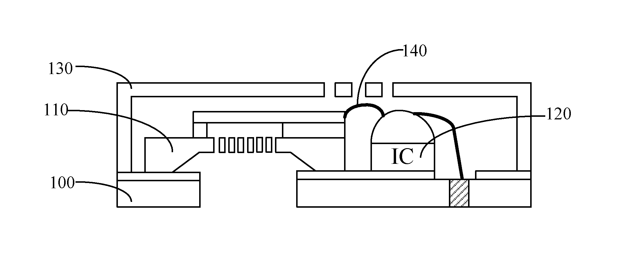
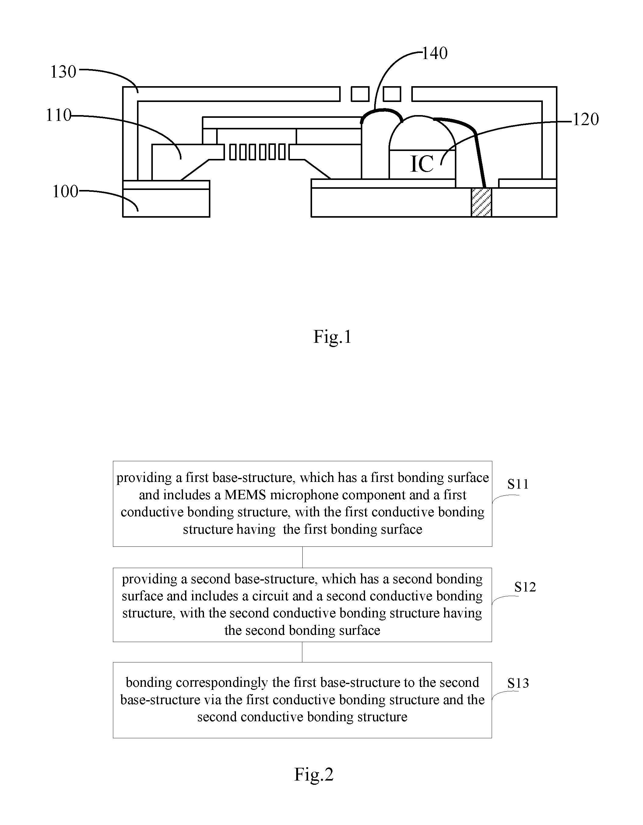
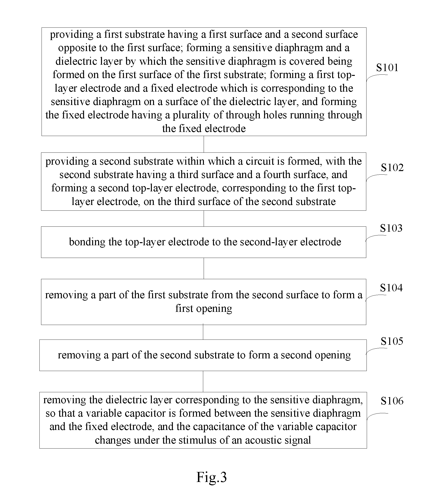
[0063]A preferred method for forming a MEMS microphone is proposed by the inventor of the present invention, referring to FIG. 3, and the method includes the following steps S101 to S106.

[0064]Step S101, providing a first substrate having a first surface and a second surface opposite to the first surface; forming a sensitive diaphragm and a dielectric layer by which the sensitive diaphragm is covered being formed on the first surface of the first substrate; forming a first top-layer electrode and a fixed electrode which is corresponding to the sensitive diaphragm on a surface of the dielectric layer, and forming the fixed electrode having a plurality of through holes running through the fixed electrode.

[0065]Step S102, providing a second substrate within which a circuit is formed, with the second substrate having a third surface and a fourth surface, and forming a second top-layer electrode, corresponding to the first top-layer electrode, on the third surface of the ...

Example

Second Embodiment

[0087]The method for forming the MEMS microphone of the present invention will be described in detail in conjunction with the second embodiment below. FIG. 4 is a schematic flowchart of a method for forming a MEMS microphone according to a second embodiment of the present invention, and the method includes the following steps S201 to S212.

[0088]Step S201, providing a first substrate having a first surface and a second surface opposite to the first surface.

[0089]Step S202, forming, on the first surface of the first substrate, a sensitive diaphragm and a plurality of interconnects.

[0090]Step S203, forming a dielectric layer by which the sensitive diaphragm and the plurality of interconnects are covered.

[0091]Step S204, forming a plurality of first through holes within the dielectric layer, with the first through holes being corresponding to the interconnect.

[0092]Step S205, forming a polycrystalline silicon layer on a surface of the dielectric layer, with the polycrys...

Example

Third Embodiment

[0163]The method for forming the MEMS microphone of the present invention will be described in detail in conjunction with the third embodiment below. FIG. 17 is a schematic flowchart of a method for forming a MEMS microphone according to a third embodiment of the present invention, and the method includes the following steps S301 to S312.

[0164]Step S301, providing a first substrate having a first surface and a second surface opposite to the first surface.

[0165]Step S302, forming, on the first surface of the first substrate, a sensitive diaphragm and a plurality of interconnects.

[0166]Step S303, forming a dielectric layer by which the sensitive diaphragm and the plurality of interconnects are covered.

[0167]Step S304, forming a plurality of first through holes within the dielectric layer, with the first through holes being corresponding to the interconnect.

[0168]Step S305, forming a polycrystalline silicon layer on a surface of the dielectric layer, with the polycrysta...


PUM

PropertyMeasurementUnit
Interferenceaaaaaaaaaa
Electrical conductoraaaaaaaaaa
Sensitivityaaaaaaaaaa

Abstract

A micro-electro-mechanical system (MEMS) microphone and a forming method therefore. The MEMS microphone comprises: a first substrate, the first substrate is provided with a first bonding face, the first substrate comprises an MEMS microphone component and a first conductive bonding structure arranged on the first bonding face, a second substrate, the second substrate is provided with a second bonding face, the second bonding substrate comprises a circuit and a second conductive bonding structure arranged on the second bonding face; the first substrate and the second substrate are oppositely fitted together via the first conductive bonding structure and the second conductive bonding structure. Embodiments of the present invention have a simple packaging technique and a compact size; the MEMS microphone packaging structure formed has a great performance on signal-to-noise ratio, and a great anti-interference capability

Description

[0001]This application claims the priority to Chinese Patent Application No. 201110061561.9, entitled “MEMS MICROPHONE AND FORMING METHOD THEREFORE”, filed with the Chinese Patent Office on Mar. 15, 2011, which is hereby incorporated by reference in its entirety.FIELD OF THE INVENTION[0002]The present invention relates to the field of micro-electro-mechanical system process, and particularly to a Micro-Electro-Mechanical Systems (MEMS) microphone and a forming method therefore.BACKGROUND OF THE INVENTION[0003]A Micro-Electro-Mechanical System (MEMS) microphone formed by a micro electronic mechanical system process has become one of the best candidates for replacing an Electret Condenser Microphone (ECM) with organic film, due to its characteristics of miniaturization and lightweight of the MEMS microphone.[0004]The MEMS microphone is a miniature microphone made by etching a pressure sensing diaphragm on a semiconductor using micro-electro-mechanical system process, and is widely use...

Claims


Application Information

Patent Timeline
IPC IPC(8): H04R23/00H04R31/00
CPCH04R23/00H04R31/00H04R1/04H04R2201/003H04R2201/029H01L2224/48091H01L2224/48137H01L2924/00014
Inventor LIU, LIANJUN
Owner MEMSEN ELECTRONICS
Why Eureka
Try Eureka