Few-layer graphene nanoribbon and a method of making the same

Inactive Publication Date: 2014-01-02
UNIV OF KENTUCKY RES FOUND
View PDF3 Cites 4 Cited by
  • Summary
  • Abstract
  • Description
  • Claims
  • Application Information

AI Technical Summary

Benefits of technology

[0011]In accordance with yet another aspect a FLG nanoribbon product is provided. That product comprises a first nanoribbon having a first chirality and a second nanoribbon also having that same first c

Problems solved by technology

However, mass producing these confining barriers to graphene at the 1 nm scale has remained elusive due to the resolution limits of standard nanolithography and other related processing techniques which are generally greater than 10 nm.
Yet the precision of electron-beam lithography (EBL) does not permit reproducible fabrication or precision at the sub-10 nm scale.
Other potential top-down techniques, such as electron-beam milling or ion-beam milling, do not provide significantly improved fabrication precision, nor (in the case electron-beam milling) the structural support required to construct the electrical components.
A major limitation of current competing top-down processing methods (such as EBL, ion beam milling, and electron beam milling) is that they do not easily align themselves to crystal orientations of the graphene.
However, these alternative methods

Method used


Image

  • Few-layer graphene nanoribbon and a method of making the same
  • Few-layer graphene nanoribbon and a method of making the same
  • Few-layer graphene nanoribbon and a method of making the same

Examples


example

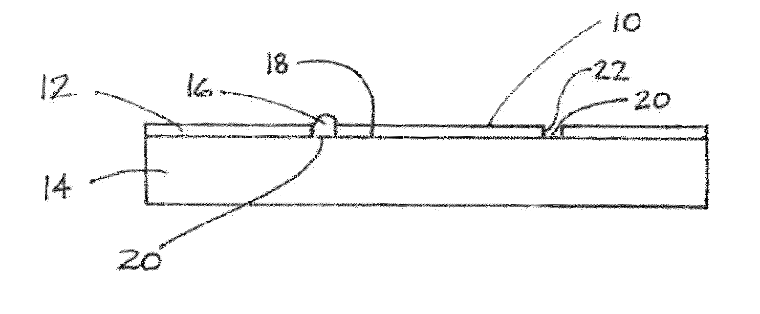
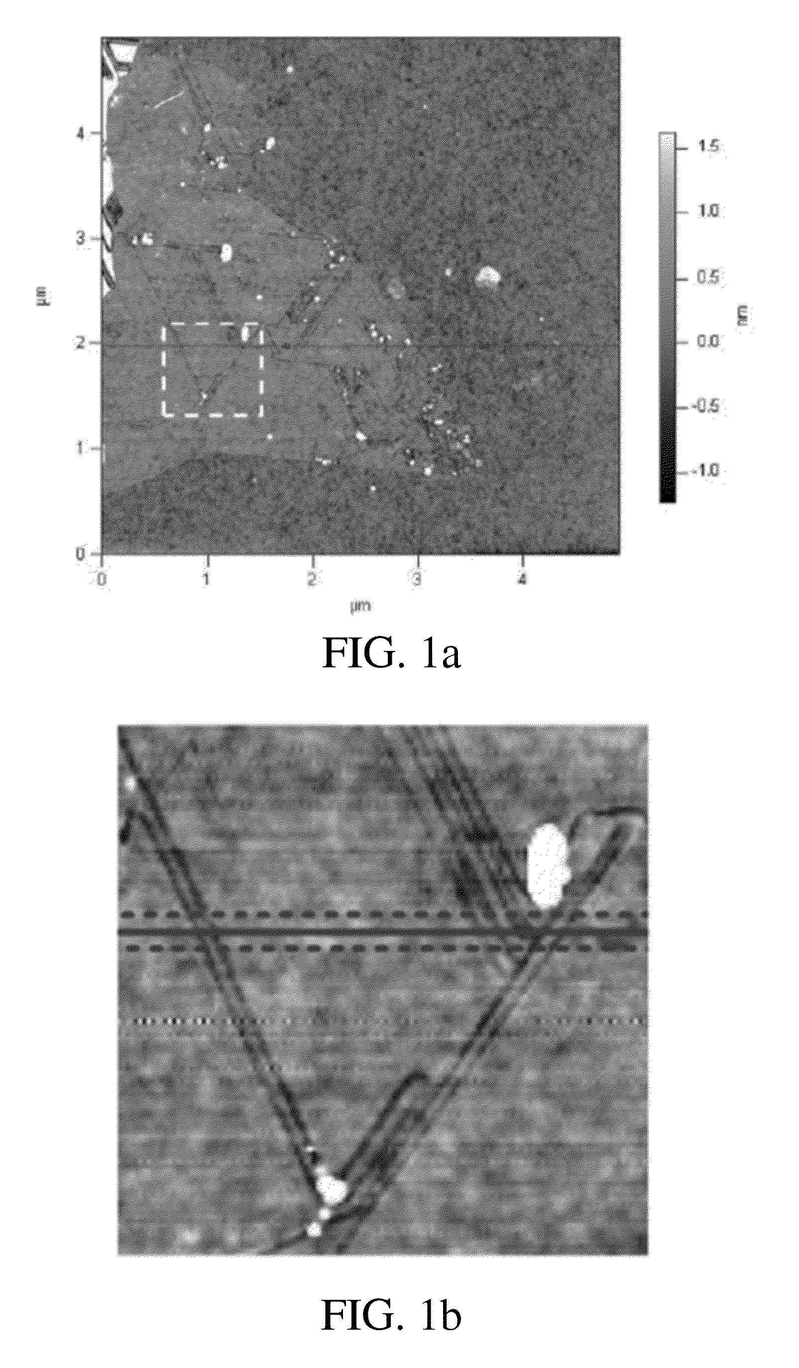
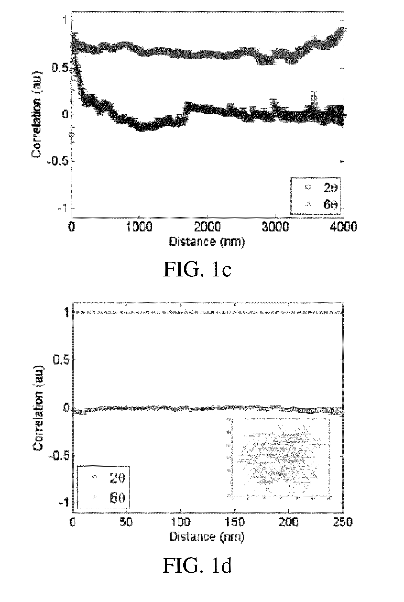
[0037]1. Graphene (SLG) or few-layer graphene (FLG) films are exfoliated, placed, or grown on an insulating or metallic substrate using well-established methods. The SLG films are ˜0.3 nm thick with FLG films of interest being N (integer) times this 0.3 nm thickness up to approximately 5 nm thick. We currently utilize exfoliated SLG and FLG samples (as described in detail below in section 1.a.), but there also exists several alternative methods (discussed in sections 1.b and 1.c). These alternative methods for SLG and FLG film fabrication, in addition to future improved methods for film fabrication on insulating or metallic substrates, could all be directly utilized for producing the invented parallel nanoribbons.[0038]1a. Exfoliated samples use a “Scotch Tape” technique that is now standard in the field of graphene sample preparation. A piece of standard Scotch Tape is pressed against a small ˜1 cm sized slab of highly order pyrolytic graphite (HOPG). The graphite is thinned by rep...


PUM

PropertyMeasurementUnit
Temperatureaaaaaaaaaa

Abstract

A method of preparing graphene nanoribbons from a few-layer graphene film includes the steps of growing or placing a few-layer graphene film on a substrate, applying nanoparticles to a surface of the few-layer graphene layer on the substrate and performing chemical vapor etching. The resulting few-layer graphene nanoribbon has a thickness of between about 0.3 nm and about 50.0 nm and a width of between about 1.0 nm and about 20.0 nm.

Description

TECHNICAL FIELD[0001]This document relates to nano-scale graphene materials and, more particularly, to graphene nanoribbons made from a few-layer graphene film.BACKGROUND SECTION[0002]Graphene is a two-dimensional material having tremendous potential use in future nano-scale electronics while also providing a wealth of novel physical properties and phenomena. Graphene's extremely high carrier mobility, two-dimensionality, and unique band structure make it a potentially ideal material for a variety of ultra-fast electronics, chemical and biological sensors, and high-current carrying devices. In particular, the electrical properties of confined graphene structures are expected to strongly depend on the orientation and nature of the confining boundaries and edges. One of the exciting prospects is that the electrical properties of graphene might be engineered through the fine control over these confining boundaries. To achieve truly engineered graphene nano-electronics it is expected th...

Claims


Application Information

Patent Timeline
IPC IPC(8): C01B31/04B05D3/10B82Y30/00B82Y40/00
CPCB82Y30/00B82Y40/00C01B2204/06C01B32/184
Inventor STRACHAN, DOUGLAS ROBERTSTIEHA, JOSEPH KELLYHUNLEY, DAVID PATRICKJOHNSON, JR., STEPHEN LEE
Owner UNIV OF KENTUCKY RES FOUND
Why Eureka
Try Eureka