Method of Manufacturing a Transparent Conductive Layer and Transparent Conductive Layer Manufactured by Same
a technology of transparent conductive layer and manufacturing method, which is applied in the direction of conductive layer on the insulating support, non-metal conductor, liquid/solution decomposition chemical coating, etc., can solve the problems of difficult mass production and size increase, large equipment cost of vacuum devices, and opaque boards such as plastic films. , to achieve the effect of excellent conductivity, low haze, and flexibility
- Summary
- Abstract
- Description
- Claims
- Application Information
AI Technical Summary
Benefits of technology
Problems solved by technology
Method used
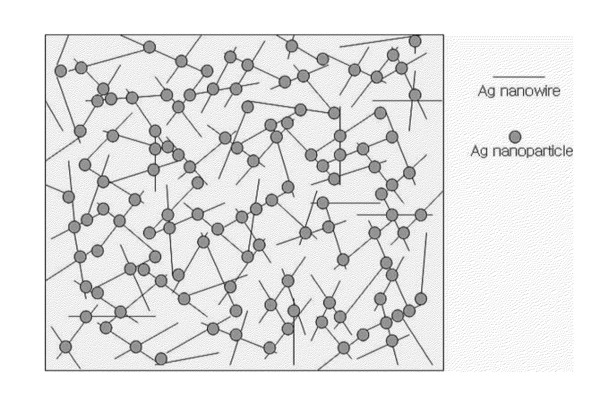
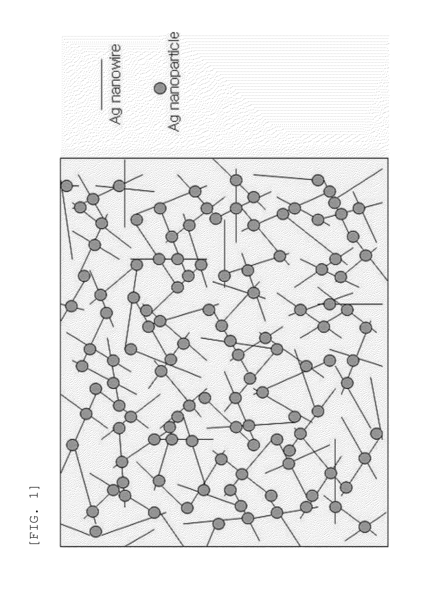
Image

Examples
example 2
Forming of Transparent Conductive Layer
[0104]Ag-1.0-NWs solution in Table 2 was dropped on polyethylene terephthalate ((PET), trademark: SH40 manufactured by SKC, light transmittance: 92%) film and coated by using a spin coater, followed by thermal treatment for 5 min at 150° C., thereby forming a primary silver nanowire layer. The above-described process was repeated once to form a secondary silver nanowire layer.
[0105]Ag Ink-0.05 solution of Table 1 was dropped on the secondary silver nanowire layer and spin-coated, followed by thermal treatment for 5 min at 150° C., thereby forming a silver nano ink layer, wherein light transmittance was 85% and surface electrical resistance was 30 Q / □.
example 3
Forming of Transparent Conductive Layer
[0106]Ag-1.0-NWs solution in Table 2 was dropped on an optical polyethylene terephthalate ((PET), trademark: SH40 manufactured by SKC, light transmittance: 92%) film and coated by using a spin coater, followed by thermal treatment for 5 min at 150° C., thereby forming a primary silver nanowire layer. The above-described process was repeated once to form a secondary silver nanowire layer.
[0107]Ag Ink-0.01 solution of Table 1 was dropped on the secondary silver nanowire layer and spin-coated, followed by thermal treatment for 5 min at 150° C., thereby forming a primary silver nano ink layer, and the above-described process was repeated once to form a secondary silver nano ink layer. Here, light transmittance was 87% and surface electrical resistance was 45 Q / □.
example 4
Forming of Transparent Conductive Layer
[0108]Ag-0.5-NWs solution in Table 2 was dropped on an optical polyethylene terephthalate ((PET), trademark: SH40 manufactured by SKC, light transmittance: 92%) film and coated by using a spin coater, followed by thermal treatment for 5 min at 150° C., thereby forming a primary silver nanowire layer. The above-described process was repeated once to form a secondary silver nanowire layer.
[0109]Ag Ink-0.05 solution of Table 1 was dropped on the secondary silver nanowire layer and spin-coated, followed by thermal treatment for 5 min at 150° C., thereby forming a primary silver nano ink layer, and the above-described process was repeated once to form a secondary silver nano ink layer. Here, light transmittance was 78% and surface electrical resistance was 20 Q / □.
PUM
| Property | Measurement | Unit |
|---|---|---|
| Temperature | aaaaa | aaaaa |
| Length | aaaaa | aaaaa |
| Length | aaaaa | aaaaa |
Abstract
Description
Claims
Application Information
 - R&D
- Intellectual Property
- Life Sciences
- Materials
- Tech Scout
- Unparalleled Data Quality
- Higher Quality Content
- 60% Fewer Hallucinations
Browse by: Latest US Patents, China's latest patents, Technical Efficacy Thesaurus, Application Domain, Technology Topic, Popular Technical Reports.
© 2025 PatSnap. All rights reserved.Legal|Privacy policy|Modern Slavery Act Transparency Statement|Sitemap|About US| Contact US: help@patsnap.com