Hydrophobic nanostructured thin films
a nanostructured, thin film technology, applied in the direction of film/foil adhesives, coatings, transportation and packaging, etc., can solve the problems of high cost, difficult preparation at industrial scale, and insufficient study of the simultaneous control of the wettability and adhesion properties of superhydrophobic surfaces
- Summary
- Abstract
- Description
- Claims
- Application Information
AI Technical Summary
Benefits of technology
Problems solved by technology
Method used
Image
Examples
example 1
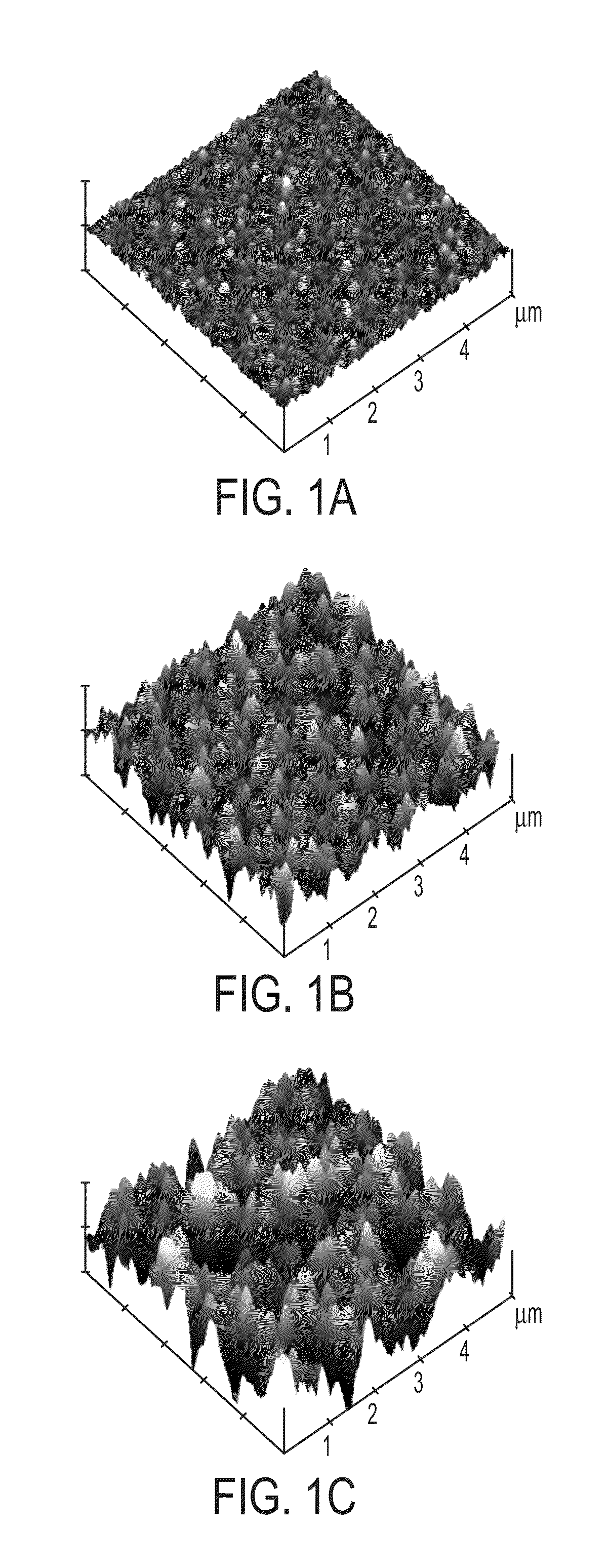
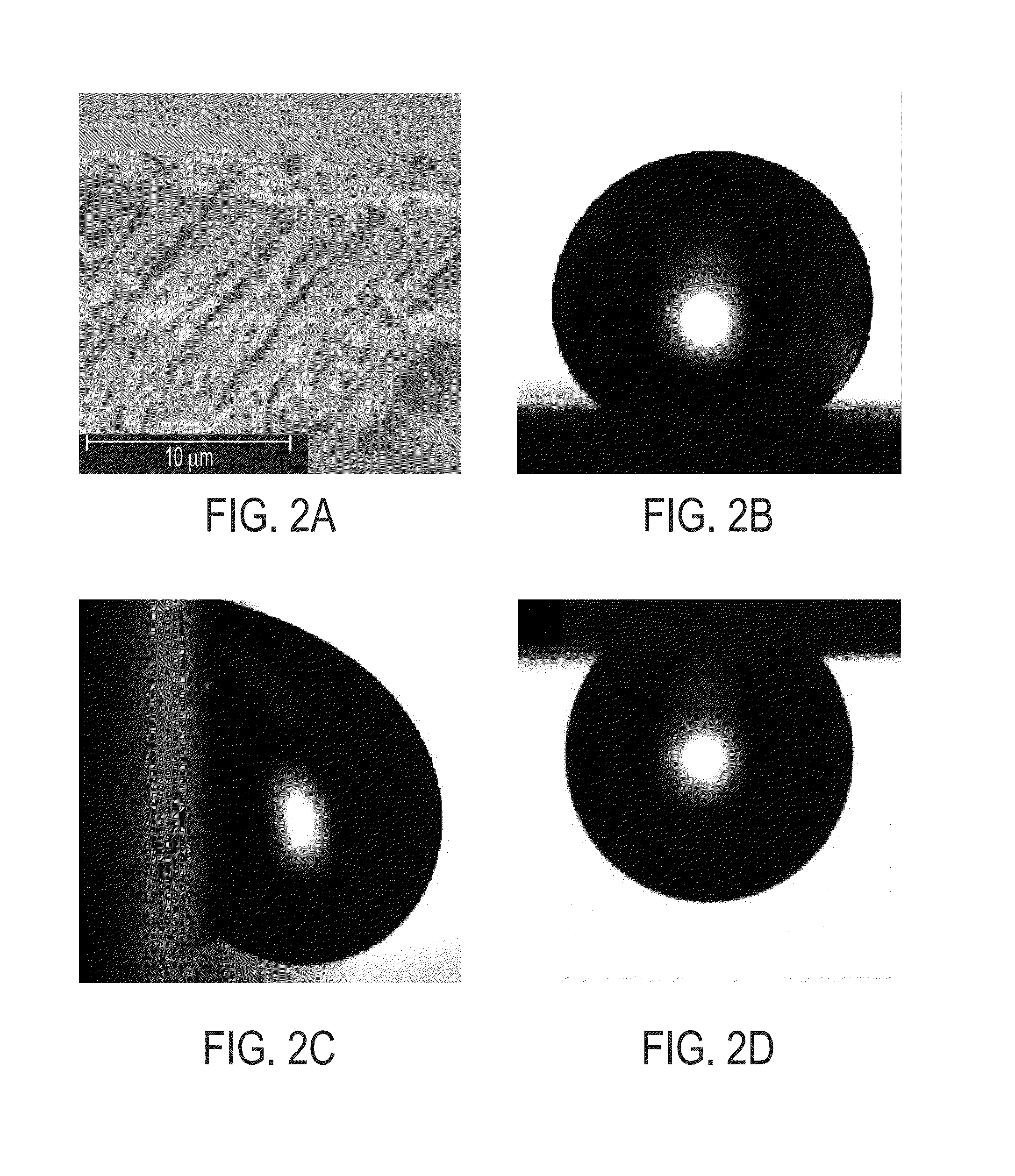
[0081]Transmission infrared spectra (IR, Bruker) were collected with respect to a silicon wafer reference in air. Spectra were recorded using Norton-Beer apodization with 1 cm−1 resolution, and for each spectrum, 400 scans were coadded. The spectra were analyzed using OPUS 5.5 software. The surface roughness was quantified by AFM (Nanoscope E, Veeco) in a liquid chamber using silicon nitride cantilevers in contact mode. Column dimensions were calculated with Nanoscope software (Veeco Metrology, CA) using the grain size tool. Contact angle measurements (DFTA 1000, First Ten Angstroms, Inc.) were carried out with a video microscope interfaced to a computer. The glancing angle XRD pattern of a nanostructured PPXC thin film deposited on a glass substrate was measured (Scintag Pad V). Samples for scanning electron microscopy (JEOL 6700F FE-SEM) images were prepared by cleaving the thin films in liquid nitrogen.
[0082]The film roughness of the nanostructured PPX fil...
example 2
PPX Film Deposition
[0084]The paracyclophane precursor for the poly(chloro-p-xylylene) (PPX-Cl) films, dichloro-di-p-xylylene, was obtained from Uniglobe-Kisco Inc. The precursors for the poly-(bromo-p-xylylene) (PPX-Br) film, dibromo-di-p-xylylene, and poly(trifluoroacetyl-p-xylylene) (PPX-COCF3) film, trifluoroacetyl-di-p-xylylene, were prepared according to the literature method (Cetinkaya et al., Polymer 2007, 48, 4130-4134). The nanocolumnar PPX films used here were prepared using an α=10° deposition angle.
example 3
Film Characterization
[0085]Static contact angles were measured by applying a video microscope interfaced to a computer (FTA-1000) to capture drop images. Deionized H2O (10 μL, 18 MΩ-cm resistivity; Barnstead Nanopure II deionizer) was used for contact angle measurements. Surface roughness was measured with a Nanoscope-E atomic force microscope (Veeco Metrology, CA) in ambient air at room temperature, with silicon nitride (SiN) triangular cantilevers having contact mode tips (DNP-20, Veeco Metrology, CA). The rms roughness from 5 μm scans (average of three sets) was calculated using the Nanoscope software without tip deconvolution methods as a result of high roughness. Scanning electron microscope (SEM) images were recorded with a Philips XL-40 system after cleaving the samples in liquid nitrogen. The FTIR (Thermo Nicolet IR) and ATR (diamond crystal) data were collected with respect to silicon wafer reference in air and were recorded using Norton-Beer apodization with 4 cm−1 resolut...
PUM
| Property | Measurement | Unit |
|---|---|---|
| water droplet roll-off angles | aaaaa | aaaaa |
| tilt angles | aaaaa | aaaaa |
| tilt angles | aaaaa | aaaaa |
Abstract
Description
Claims
Application Information


