Semiconductor device

a technology of semiconductors and devices, applied in the direction of semiconductor devices, electrical devices, transistors, etc., can solve the problems of increased power consumption of cpu, so as to achieve convenient and fast operation, favorable electrical characteristics, and favorable reliability

Active Publication Date: 2014-01-30
SEMICON ENERGY LAB CO LTD
View PDF15 Cites 35 Cited by
  • Summary
  • Abstract
  • Description
  • Claims
  • Application Information

AI Technical Summary

Benefits of technology

[0027]In general, as a formed film becomes denser, the refractive index of the film is increased and the etching rate of the film is reduced. Accordingly, by forming the second nitride insulating film using a nitride insulating film having a refractive index and an etching rate in the above ranges, the second nitride insulating film can be a dense film, so that the second nitride insulating film can exhibit a barrier property against hydrogen. Further, as a formed film becomes denser, the density of the film is increased; therefore, in order that the second nitride insulating film can sufficiently exhibit a barrier property against hydrogen, the second nitride insulating film is preferably formed using a nitride insulating film having a density in the above range.
[0040]According to one embodiment of the present invention, a semiconductor device which has favorable reliability by using a transistor including a silicon semiconductor and a transistor including an oxide semiconductor can be provided.

Problems solved by technology

As a result, the power consumption of the CPU is increased.
The hydrogenation treatment is performed by heat treatment in a hydrogen atmosphere, an ion implantation method, an ion doping method, or the like and has problems in view of treatment time, safety, cost, and the like.

Method used


Image

  • Semiconductor device
  • Semiconductor device
  • Semiconductor device

Examples


embodiment 1

[0074]In the present embodiment, a semiconductor device that is one embodiment of the present invention is described with reference to drawings.

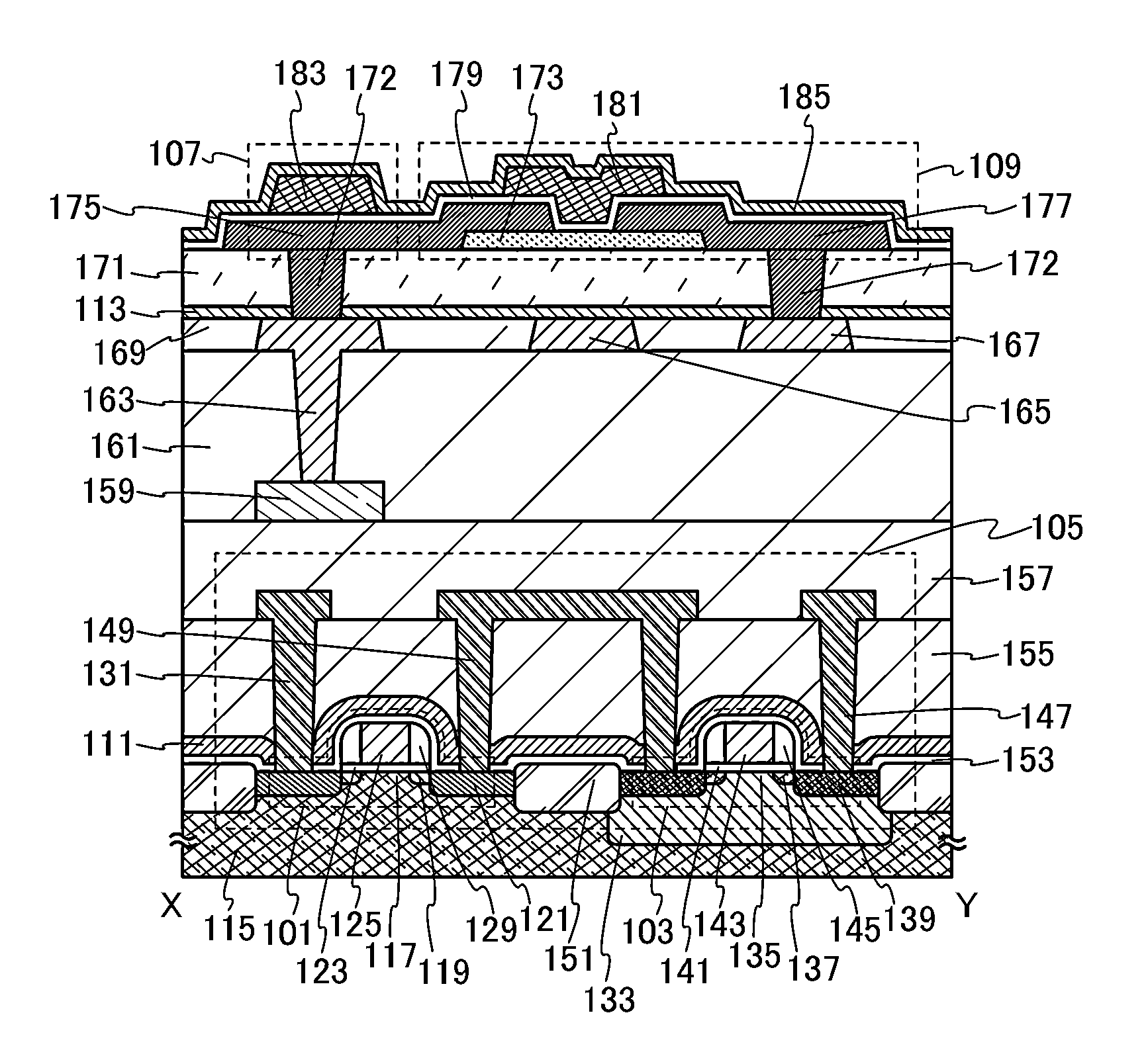
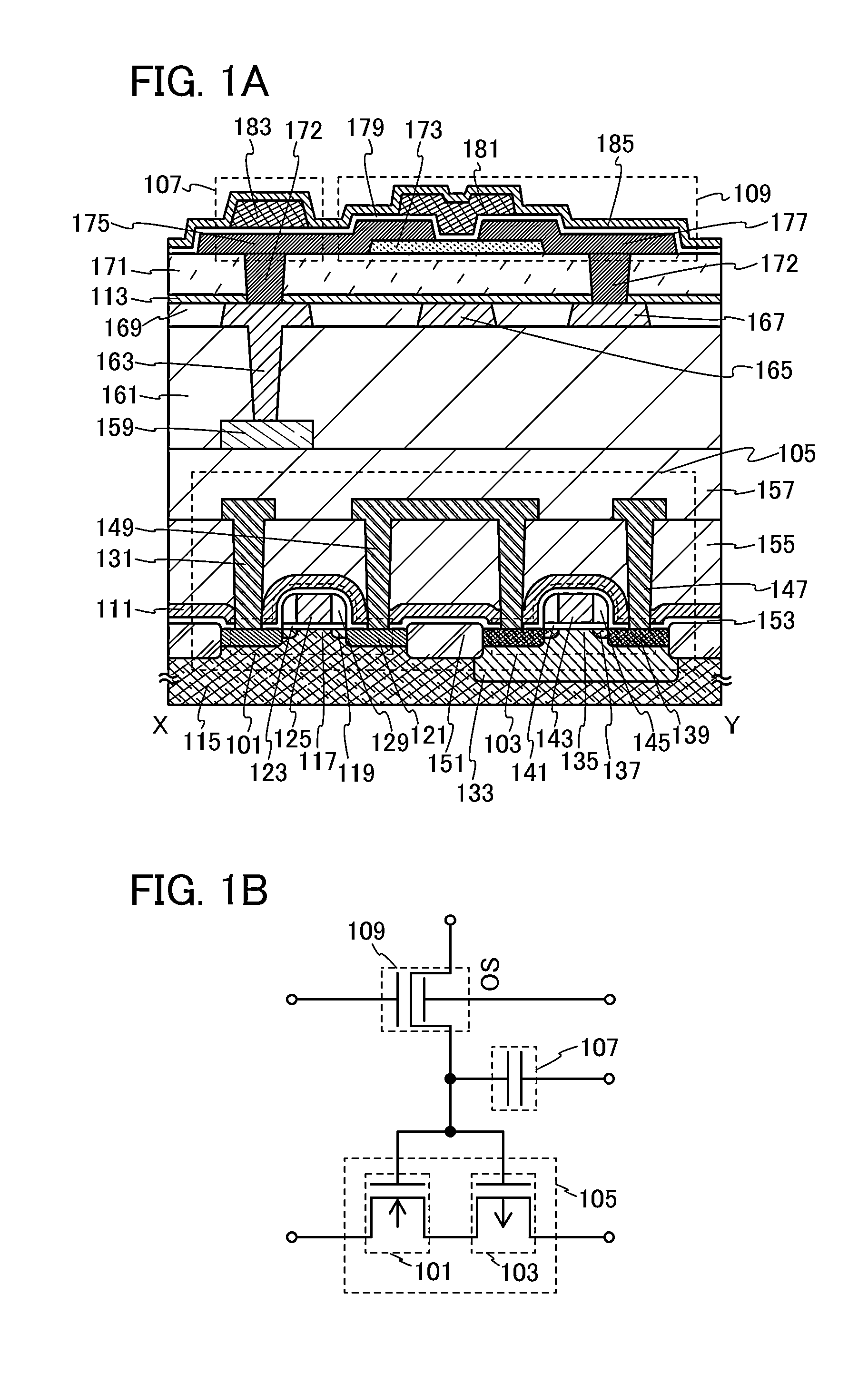
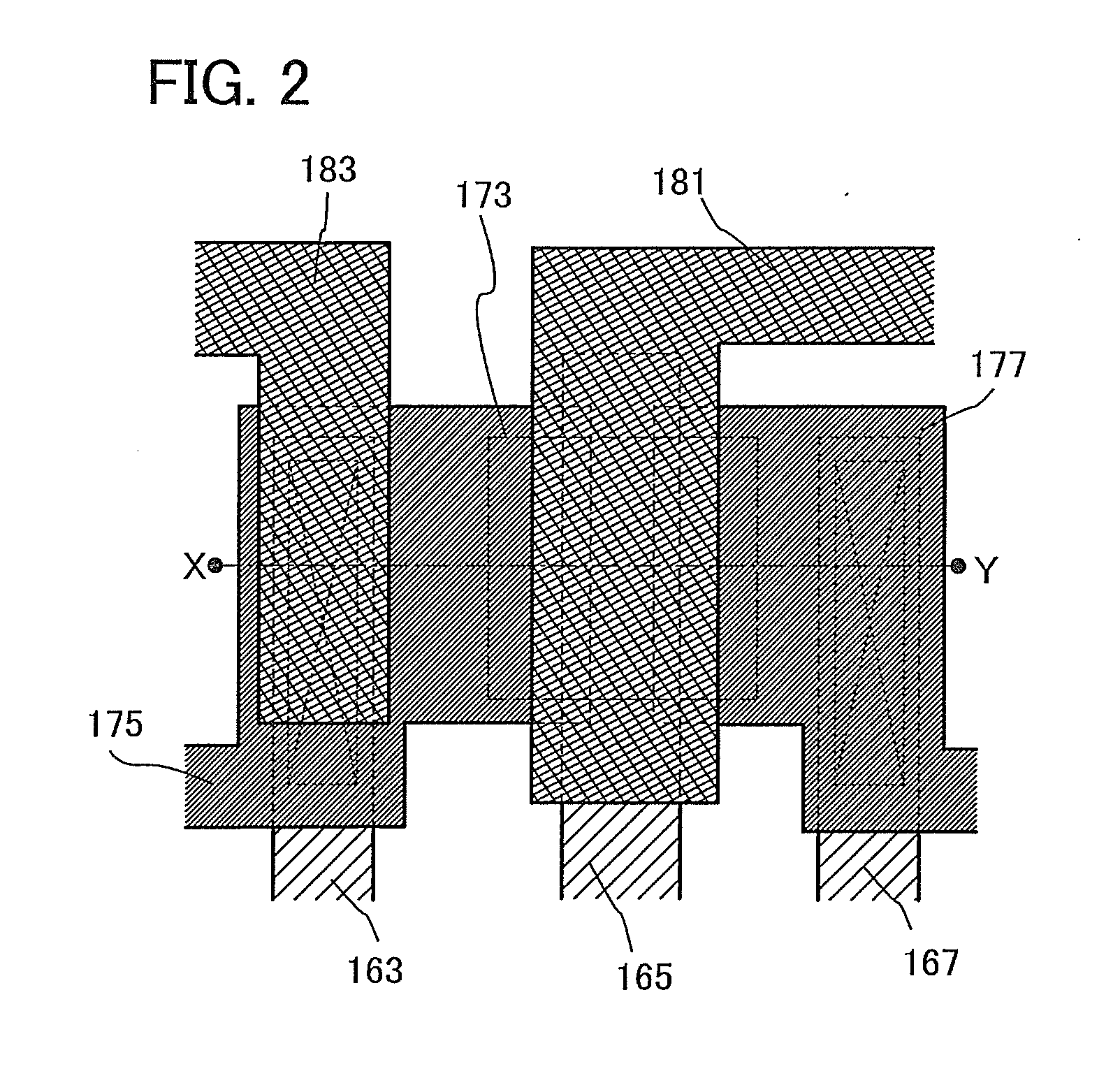
[0075]FIG. 1A is a cross-sectional view illustrating a semiconductor device that is one embodiment of the present invention. The semiconductor device illustrated in FIG. 1A includes a plurality of transistors, and some of the transistors are stacked in the longitudinal direction in order to increase the degree of integration.

[0076]Specifically, a complementary metal oxide semiconductor (CMOS) circuit 105 in which a transistor 101 that is an n-channel transistor including a first semiconductor material and a transistor 103 that is a p-channel transistor are electrically connected to each other is provided in a lower portion; a capacitor 107 and a transistor 109 that is an n-channel transistor including a second semiconductor material are provided over the CMOS circuit 105; a first nitride insulating film 111 which contains hydrogen and releas...

embodiment 2

[0216]As another example of the semiconductor device that is one embodiment of the present invention, an example of a cross-sectional view of a NOR circuit, which is a logic circuit, is illustrated in FIG. 11A. FIG. 11B is a circuit diagram of the NOR circuit in FIG. 11A, and FIG. 11C is a circuit diagram of a NAND circuit.

[0217]FIG. 11A is a cross-sectional view of part of the NOR circuit, specifically, a cross-sectional view of transistors 202 and 203 which are a p-channel transistor and an n-channel transistor, respectively. FIG. 12 is a top view of the part of the NOR circuit. The cross-sectional view illustrated in FIG. 11A corresponds to a cross section taken along a dashed dotted line X-Y in the top view in FIG. 12. In the top view in FIG. 12, some components (the transistor 202, a first nitride insulating film 211, a second nitride insulating film 213, other gate insulating films and interlayer insulating films, and the like) are not illustrated for clarification of the draw...

embodiment 3

[0256]In this embodiment, an example of an oxide semiconductor film which is applicable to an oxide semiconductor film in a transistor including an oxide semiconductor which is applicable to the semiconductor device described in any of the semiconductor devices in the above embodiments is described.

[0257]Besides an amorphous oxide semiconductor, a single crystal oxide semiconductor, and a polycrystalline oxide semiconductor, an oxide semiconductor including crystal parts (c-axis aligned oxide semiconductor: CAAC-OS) is preferably used for an oxide semiconductor film in the transistor including an oxide semiconductor.

[0258]The CAAC-OS is one of oxide semiconductor films including a plurality of crystal parts, and most of each crystal part fits inside a cube whose one side is less than 100 nm. Thus, there is a case where a crystal part included in the CAAC-OS film fits a cube whose one side is less than 10 nm, less than 5 nm, or less than 3 nm. The density of defect states of the CAAC...


PUM


Abstract

A nitride insulating film which prevents diffusion of hydrogen into an oxide semiconductor film in a transistor including an oxide semiconductor is provided. Further, a semiconductor device which has favorable electrical characteristics by using a transistor including a silicon semiconductor and a transistor including an oxide semiconductor is provided. Two nitride insulating films having different functions are provided between the transistor including a silicon semiconductor and the transistor including an oxide semiconductor. Specifically, a first nitride insulating film which contains hydrogen is provided over the transistor including a silicon semiconductor, and a second nitride insulating film which has a lower hydrogen content than the first nitride insulating film and functions as a barrier film against hydrogen is provided between the first nitride insulating film and the transistor including an oxide semiconductor.

Description

BACKGROUND OF THE INVENTION[0001]1. Field of the Invention[0002]The invention disclosed in this specification and the like relates to a semiconductor device including transistors and further relates to a nitride insulating film included in the semiconductor device.[0003]2. Description of the Related Art[0004]In recent years, technical development on high-speed operation of semiconductor devices including central processing units (also referred to as CPUs) and the like has been actively conducted. CPUs include semiconductor integrated circuits including logic circuits. Semiconductor integrated circuits include transistors, memories, and electrodes serving as connection terminals, which are formed over semiconductor wafers.[0005]As technical development on high-speed operation, semiconductor elements such as transistors are reduced in size to improve the operation speed and the degree of integration of CPUs.[0006]By a reduction in size of a semiconductor element such a transistor, the...

Claims


Application Information

Patent Timeline
Patent Type & Authority Applications(United States)
IPC IPC(8): H01L27/088
CPCH01L27/088H01L27/0688H01L27/1225H01L27/0617H01L27/1207
Inventor YAMAZAKI, SHUNPEITANAKA, TETSUHIROIEDA, YOSHINORIMIYAMOTO, TOSHIYUKINOMURA, MASAFUMIHAMOCHI, TAKASHIOKAZAKI, KENICHIICHIJO, MITSUHIROENDO, TOSHIYA
Owner SEMICON ENERGY LAB CO LTD
Why Eureka
Try Eureka