Method for forming thin metal compound film and semiconductor structure with thin metal compound film

a technology thin metal compound film, which is applied in the direction of semiconductor devices, electrical equipment, basic electric elements, etc., can solve the problems of difficult control of the thickness of metal silicide film, adverse high-temperature annealing, and unsatisfactory performance, so as to enhance the performance of the semiconductor device and reduce the resistance of the sh

Inactive Publication Date: 2014-01-30
NAT APPLIED RES LAB
View PDF5 Cites 4 Cited by
  • Summary
  • Abstract
  • Description
  • Claims
  • Application Information

AI Technical Summary

Benefits of technology

[0007]In accordance with an aspect of the present invention, a method for forming an extremely thin metal film with low sheet resistance in a semiconductor device is provided in order to enhance the performance of the semiconductor device. In an embodiment, a substrate structure is provided. Then a first metal layer is formed on the substrate structure. After that, a first microwave annealing (MWA) process is performed to conduct a reac...

Problems solved by technology

Thus production of a semiconductor device, such as a metal-oxide-semiconductor field effect transistor (MOSFET), with deep submicron meter size faces a bottleneck in miniaturization due to unsatisfactory performance.
As known to those skilled in the art, high-temperature annealing is adverse to the fabrication of a MOSFET with deep submicron meter size as metal...

Method used


Image

  • Method for forming thin metal compound film and semiconductor structure with thin metal compound film
  • Method for forming thin metal compound film and semiconductor structure with thin metal compound film
  • Method for forming thin metal compound film and semiconductor structure with thin metal compound film

Examples


Embodiment Construction

[0030]The present invention will now be described more specifically with reference to the following embodiments. It is to be noted that the following descriptions of preferred embodiments of this invention are presented herein for purpose of illustration and description only. It is not intended to be exhaustive or to be limited to the precise form disclosed.

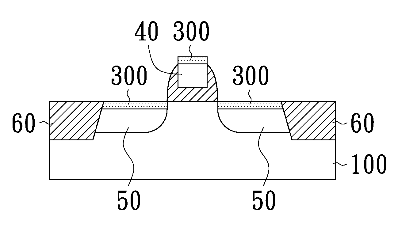
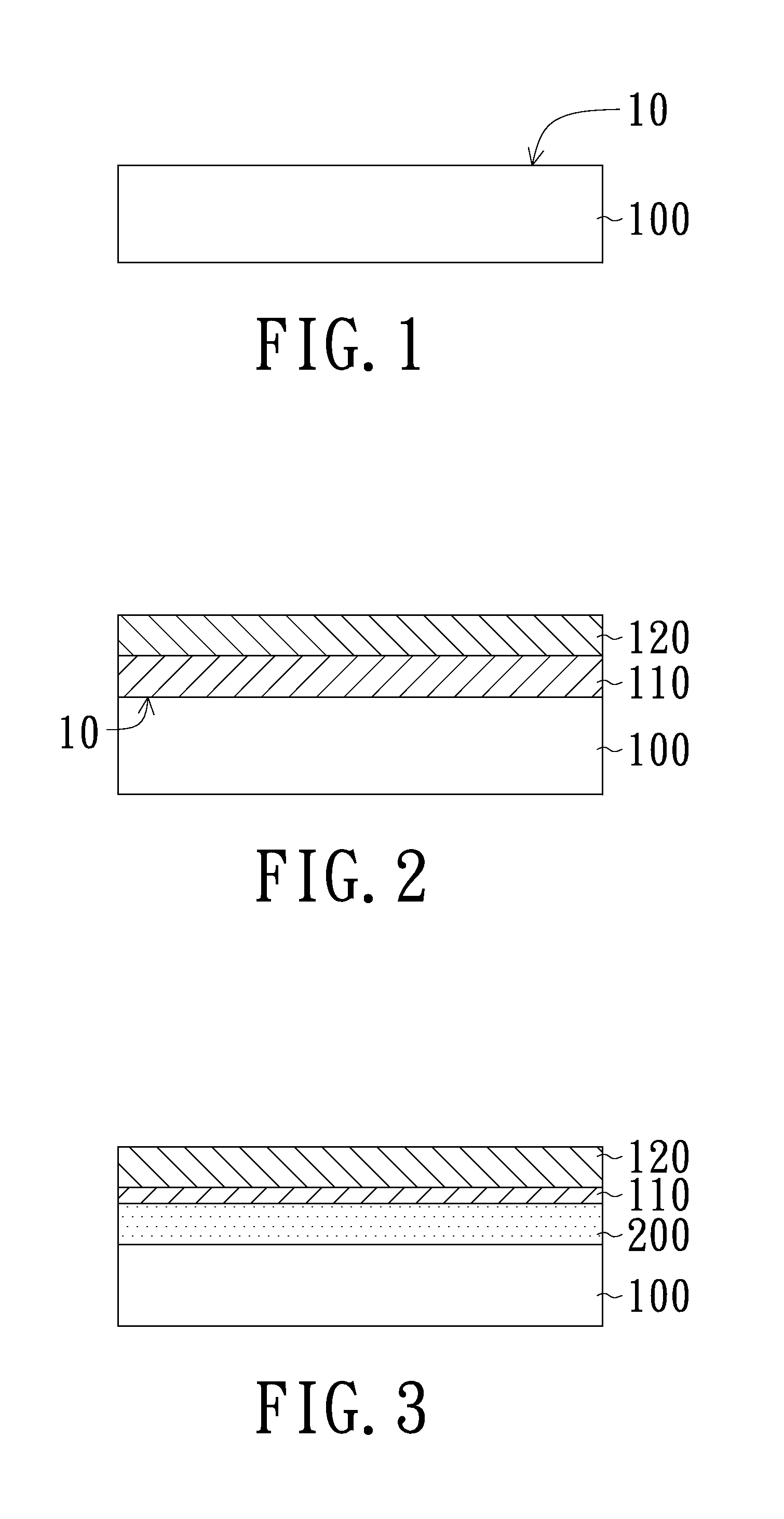
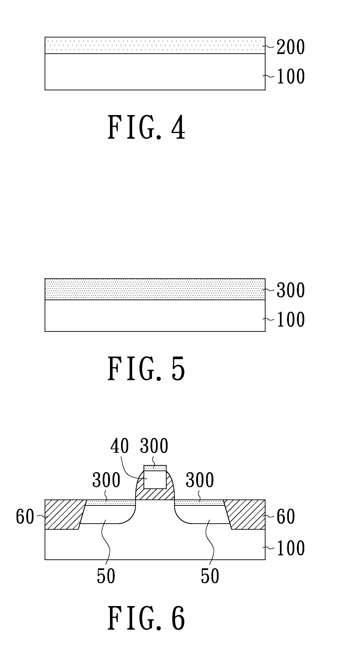
[0031]With reference to FIGS. 1 to 6, a method for forming a semiconductor structure having a metal compound in accordance with an embodiment of the present invention and the resulting semiconductor structure are schematically illustrated. Firstly, a first metal layer 110 is deposited on a surface 10 of a substrate 100. In this embodiment, before the SALICIDE process, the surface 10 of the substrate 100 has been formed thereon a gate region 40, a source / drain region 50 and shallow trench isolations 60 (FIGS. 1 and 6). The first metal layer 110 is then directly deposited on the gate region and the source / drain regions. Electronic ...


PUM


Abstract

A method for forming a metal compound film includes: providing a substrate structure; forming a first metal layer on the substrate structure; performing a first microwave annealing process to conduct a reaction between the first metal layer and the substrate structure so as to form a first polycrystalline film of a metal compound; and performing a second microwave annealing process to transform the first polycrystalline film into a second polycrystalline film of the metal compound with an enlarged grain size, wherein a microwave power output used in the second microwave annealing process is higher than that used in the first microwave annealing process.

Description

BACKGROUND OF THE INVENTION[0001]1. Field of the Invention[0002]The present invention relates to a method for forming a thin metal compound film, and more particularly, to a method for forming a thin metal compound film in a semiconductor device. The present invention also relates to a semiconductor structure having a thin metal compound film.[0003]2. Description of Related Art[0004]The miniaturization of a semiconductor device inherently leads to an increase in sheet resistance of the device. Thus production of a semiconductor device, such as a metal-oxide-semiconductor field effect transistor (MOSFET), with deep submicron meter size faces a bottleneck in miniaturization due to unsatisfactory performance.[0005]In a common process for fabricating a semiconductor chip, a self-align silicide (SALICIDE) process is used to form metal silicide films on gate and source / drain regions of a MOSFET. The conventional SALICIDE process involves two stages of rapid thermal annealing (RTA). The fi...

Claims


Application Information

Patent Timeline
IPC IPC(8): H01L29/40
CPCH01L29/40H01L29/401H01L21/28052H01L21/28255H01L21/28264H01L21/28518H01L21/324H01L29/665
Inventor LEE, YAO-JENHSUEH, FU-KUOSUNG, PO-JUNGHEH, DA-WEIHOU, FU-JULO, CHIH-HUNGCHEN, HSIU-CHIH
Owner NAT APPLIED RES LAB
Why Eureka
Try Eureka