Three-dimensional integrated circuit laminate, and interlayer filler for three-dimensional integrated circuit laminate
Active Publication Date: 2014-01-30
MITSUBISHI CHEM CORP
View PDF6 Cites 16 Cited by
Summary
Abstract
Description
Claims
Application Information
AI Technical Summary
This helps you quickly interpret patents by identifying the three key elements:
Problems solved by technology
Method used
Benefits of technology
Benefits of technology
The present invention relates to a method of making a three-dimensional integrated circuit laminate with high reliability. This is achieved by laminating semiconductor substrates each with a semiconductor device layer formed thereon by an interlayer filler layer with high thermal conductivity, low dielectric constant, and low linear thermal expansion property. The lamination accelerates thermal conductivity between the semiconductor substrates and reduces the temperature of the semiconductor device substrates, resulting in a high dissipation property and high speed operation of the semiconductor device. This allows for a stable operation of the semiconductor device.
Problems solved by technology
For practical use of such a three-dimensional integrated circuit device, various problems have been pointed out.
One of them is a problem of dissipation of heat generated from a device such as a transistor or wiring.
This problem results from a commonly very low thermal conductivity of an interlayer filler composition to be used for lamination of semiconductor substrates as compared with metals and ceramics, and there are concerns about a decrease in the performance such as malfunction of a semiconductor device due to accumulation of heat in a laminate of the semiconductor substrates.
As a further problem, the coefficient of linear thermal expansion required for the interlayer filler composition varies depending upon the difference in the structure of a laminate of the semiconductor substrates.
As another problem, there is a problem of the dielectric constant of the interlayer filler composition to be used for lamination of a semiconductor device.
On that occasion, if the dielectric constant of an interlayer filler composition to be used for lamination of a semiconductor device is high, signal transmission delays in wiring between substrates will occur, thus leading to a decrease in the operating speed of the entire device.
On the other hand, in a three-dimensional integrated circuit laminate having the semiconductor substrate laminate further bonded to an organic substrate, to an interlayer filler layer formed between the semiconductor substrate laminate and the organic substrate, a potential stress is applied due to a difference in the coefficient of linear thermal expansion by heat between the semiconductor substrates and the organic substrate, and accordingly if the interlayer filler layer does not have an appropriate coefficient of linear thermal expansion, destruction of the semiconductor device layer, breakage of the electric signal connection terminal, or the like may occur in some cases.
Method used
Image
Click on the blue label to locate the original text in one second.
Reading with bidirectional positioning of images and text.
Examples
example 1
[0246]45 parts by weight of epoxy resin (A2-1), 5 parts by weight of reactive diluting agent (A4) and 50 parts by weight of inorganic filler (B-1) were mixed, and the mixture was passed through a three-roll mill of which the roll distance was adjusted to 10 μm five times to obtain a mixture paste of the epoxy resin / the inorganic filler.
[0247]The average particle size of the inorganic filler (B-1) in the mixture paste of the epoxy resin / the inorganic filler was 0.6 μm. Further, the specific surface area of the inorganic filler (B-1) was 9.69 m2 / g.
[0248]5 parts by weight of curing agent (C-1) was added to 100 parts by weight of the mixture paste of the epoxy resin / the inorganic filler, followed by mixing by a rotary and revolutionary mixing apparatus (“Awatori Rentaro”, tradename, manufactured by THINKY CORPORATION) at 2,000 revolutions under conditions of mixing for 5 minutes and bubble removal for one minute.
[0249]The mixed paste was sandwiched between glass plates subjected to rele...
example 2
[0250]The same operation as in Example 1 was carried out except that inorganic filler (B-2) was used instead of inorganic filler (B-1) in Example 1.
[0251]The average particle size of the inorganic filler (B-2) by the above measurement method was 4.1 μm. Further, the specific surface area of the inorganic filler (B-2) was 16 m2 / g.
[0252]Of the obtained interlayer filler composition film, the thermal conductivity was 0.5 W / (m·K) and the dielectric constant was 3.2. Further, the dielectric constant was calculated from the volume fraction of the filler component in the interlayer filler composition based on the dielectric constants (epoxy resin: 2.8, boronnitride: 3.9) of the respective materials.
example 3
[0253]As epoxy resin (A), 5 g of the epoxy resin (A1) solution, 3.75 g of epoxy resin (A2-2), 0.94 g (80 wt % cyclohexanone solution) of epoxy resin (A2-3), 2.14 g (70 wt % cyclohexanone solution) of epoxy resin (A2-4), 7.24 g of inorganic filler (B-1) and further, 24.0 g of zirconia balls (YTZ-2) having a diameter of 2 mm were added, followed by stirring by a rotary and revolutionary stirring machine at 2,000 rpm for 33 minutes. After completion of stirring, the beads were removed by filtration, and 0.15 g of curing agent (C-2) and 0.15 g of flux (D-1) were added, followed by further stirring by a rotary and revolutionary stirring machine for 6 minutes to obtain an interlayer filler paste (coating fluid).
[0254]The particle size distribution of inorganic filler (B-1) in the obtained interlayer filler paste after stirring was measured, whereupon the average particle size was 1.0 μm and the maximum particle size was 5.9 μm.
[0255]This material paste was applied to a glass substrate sub...
PUM
Property
Measurement
Unit
Length
aaaaa
aaaaa
Length
aaaaa
aaaaa
Length
aaaaa
aaaaa
Abstract
To provide a three-dimensional integrated circuit laminate filled in with an interlayer filler composition having both high thermal conductivity and low linear expansion property.A three-dimensional integrated circuit laminate, which comprises a semiconductor substrate laminate having at least two semiconductor substrates each having a semiconductor device layer formed thereon laminated, and has a first interlayer filler layer containing a resin (A) and an organic filler (B) and having a thermal conductivity of at least 0.8 W / (m·K) between the semiconductor substrate.
Description
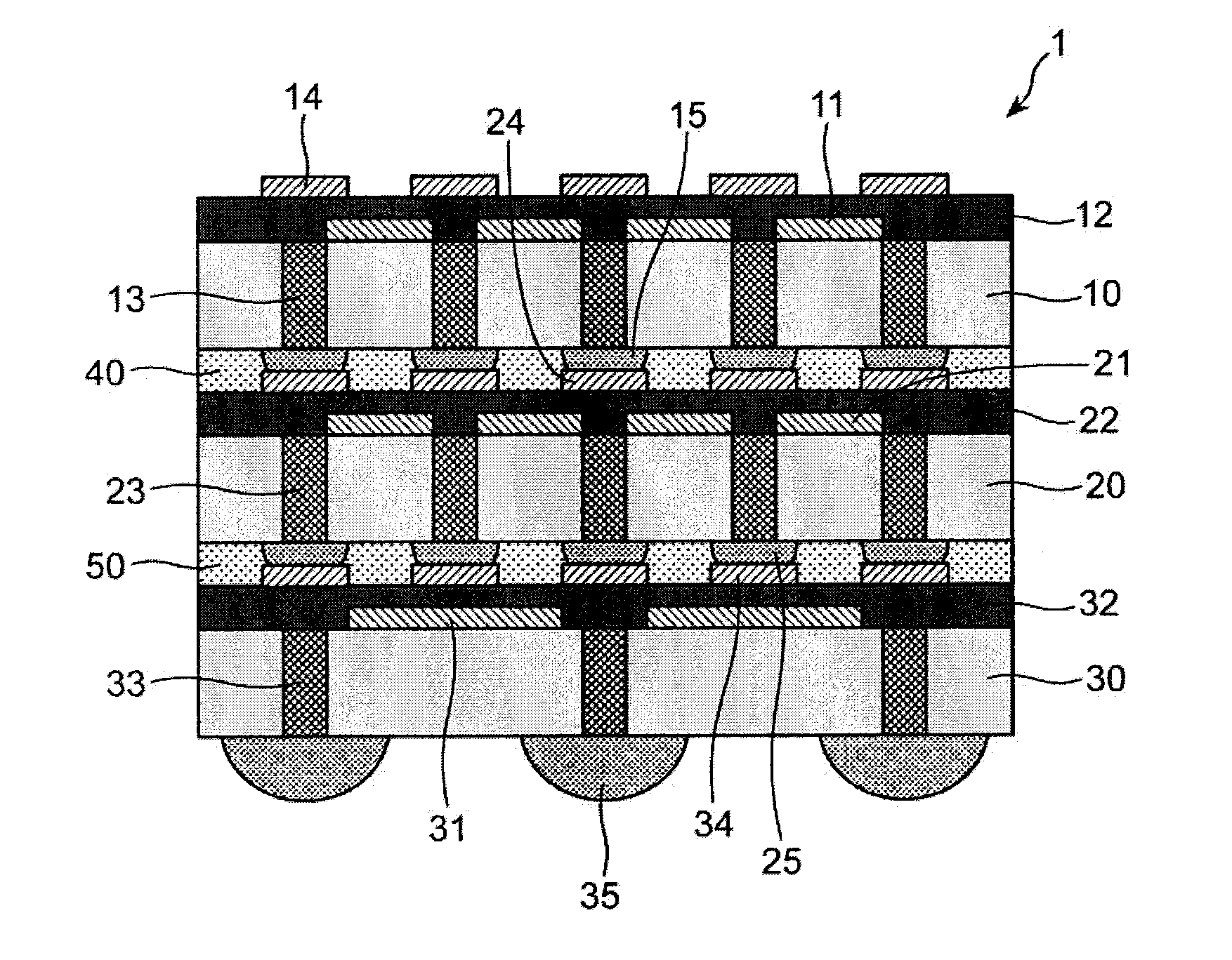
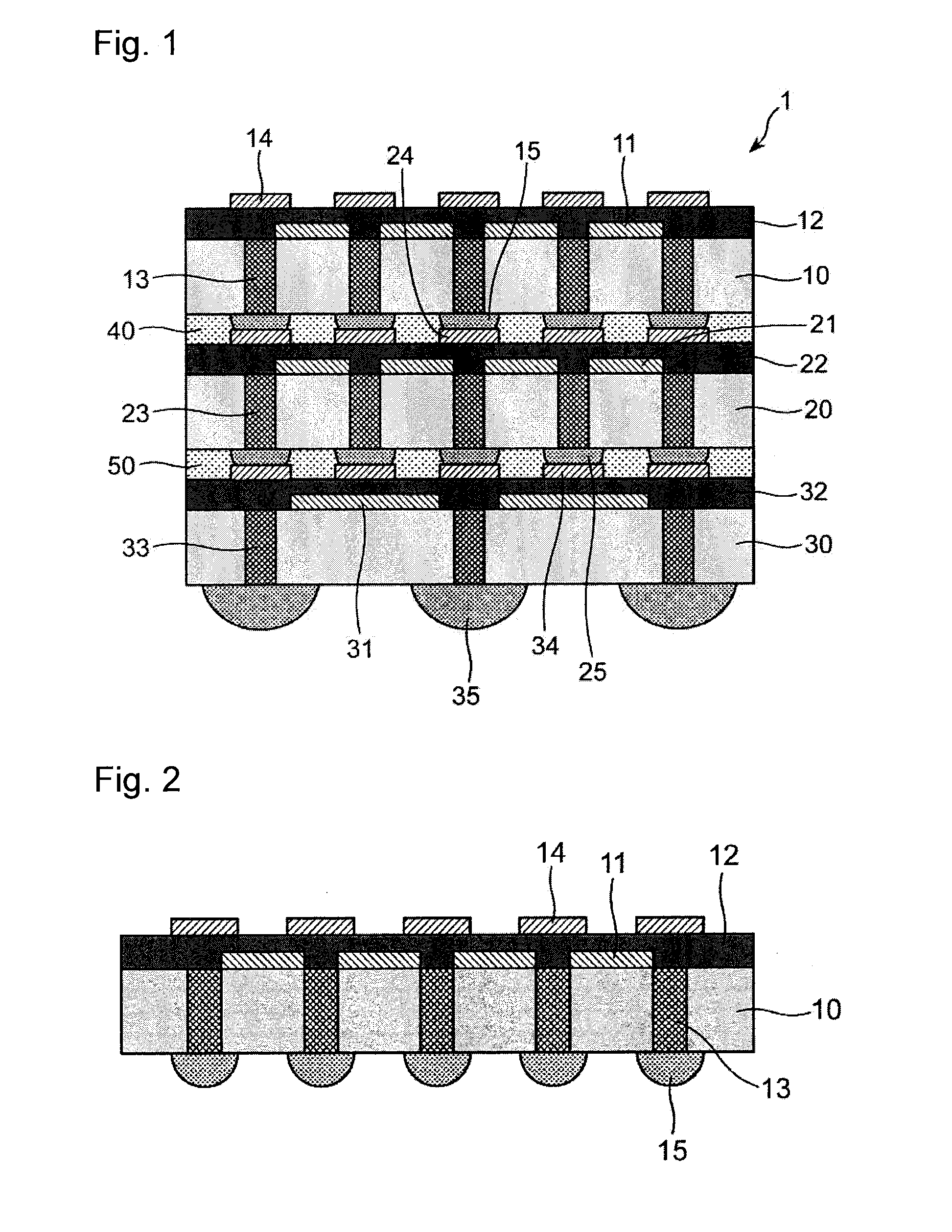
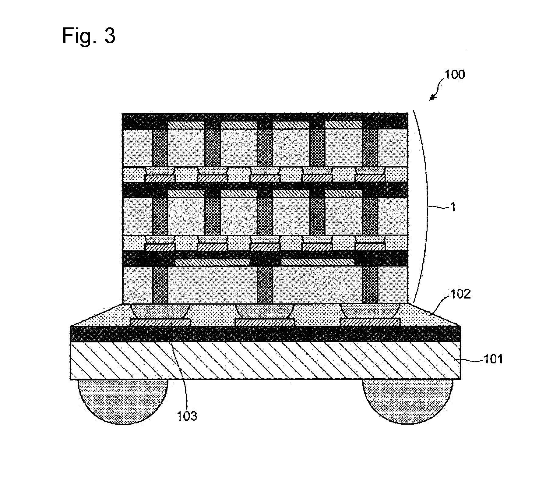
TECHNICAL FIELD[0001]The present invention relates to a three-dimensional integrated circuit laminate having semiconductor substrates laminated, and an interlayer filler for a three-dimensional integrated circuit laminate.BACKGROUND ART[0002]In recent years, for further improvement in the performance of semiconductor devices such as speeding up and an increase in the capacity, research and development is in progress to improve the performance by a three-dimensional (3D) lamination having at least two semiconductor substrates laminated, in addition to refinement of transistors and wiring.[0003]Specifically, such a process is proposed (non-Patent Documents 1 and 2) that a thin film of an interlayer filler composition is formed by an underfilling process of pouring a filler from the side of semiconductor substrates after bonding of the substrates or by application to a wafer, and then B-stage formation is carried out, then semiconductor substrates are cut out by dicing (wafercutting),...
Claims
Application Information
Patent Timeline
Application Date:The date an application was filed.
Publication Date:The date a patent or application was officially published.
First Publication Date:The earliest publication date of a patent with the same application number.
Issue Date:Publication date of the patent grant document.
PCT Entry Date:The Entry date of PCT National Phase.
Estimated Expiry Date:The statutory expiry date of a patent right according to the Patent Law, and it is the longest term of protection that the patent right can achieve without the termination of the patent right due to other reasons(Term extension factor has been taken into account ).
Invalid Date:Actual expiry date is based on effective date or publication date of legal transaction data of invalid patent.

