Method for forming copper wiring
a technology of copper wiring and copper wire, which is applied in the direction of vacuum evaporation coating, semiconductor/solid-state device details, coatings, etc., can solve the problems of insufficient reliability, void in the interface, and insufficient strength, and achieve good adhesion to the cap layer and low wiring resistance.
- Summary
- Abstract
- Description
- Claims
- Application Information
AI Technical Summary
Benefits of technology
Problems solved by technology
Method used
Image

Examples
first embodiment
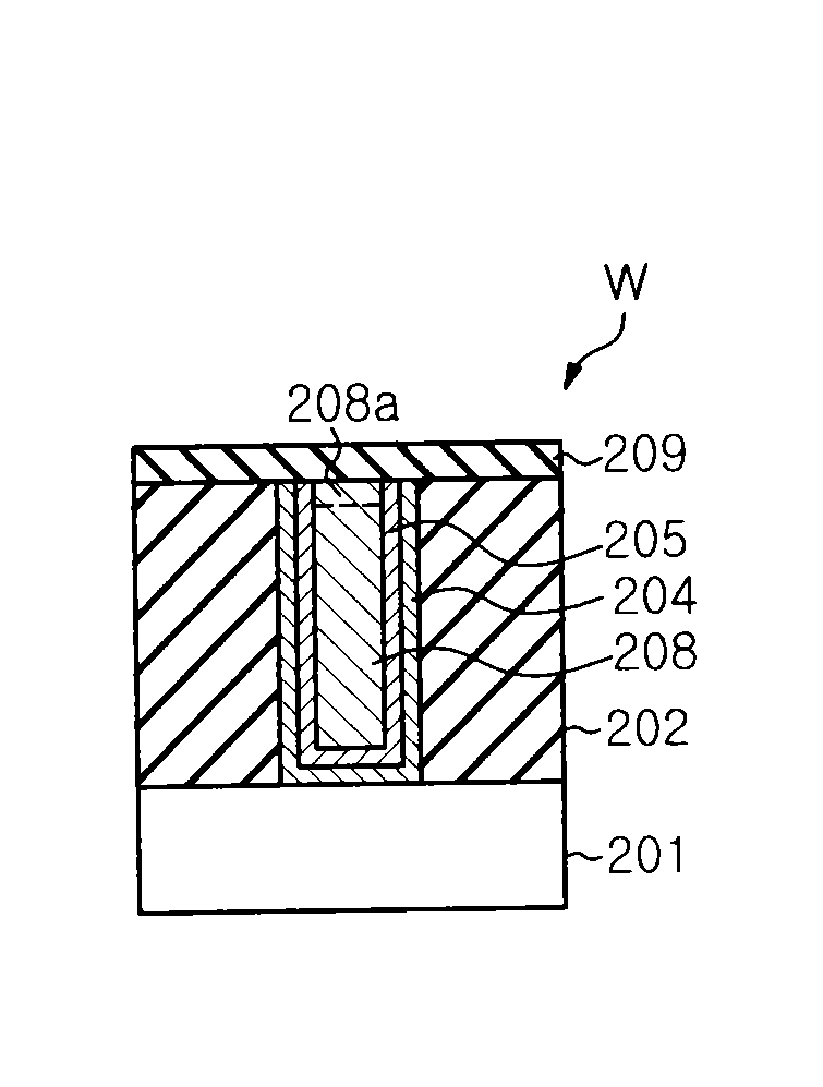
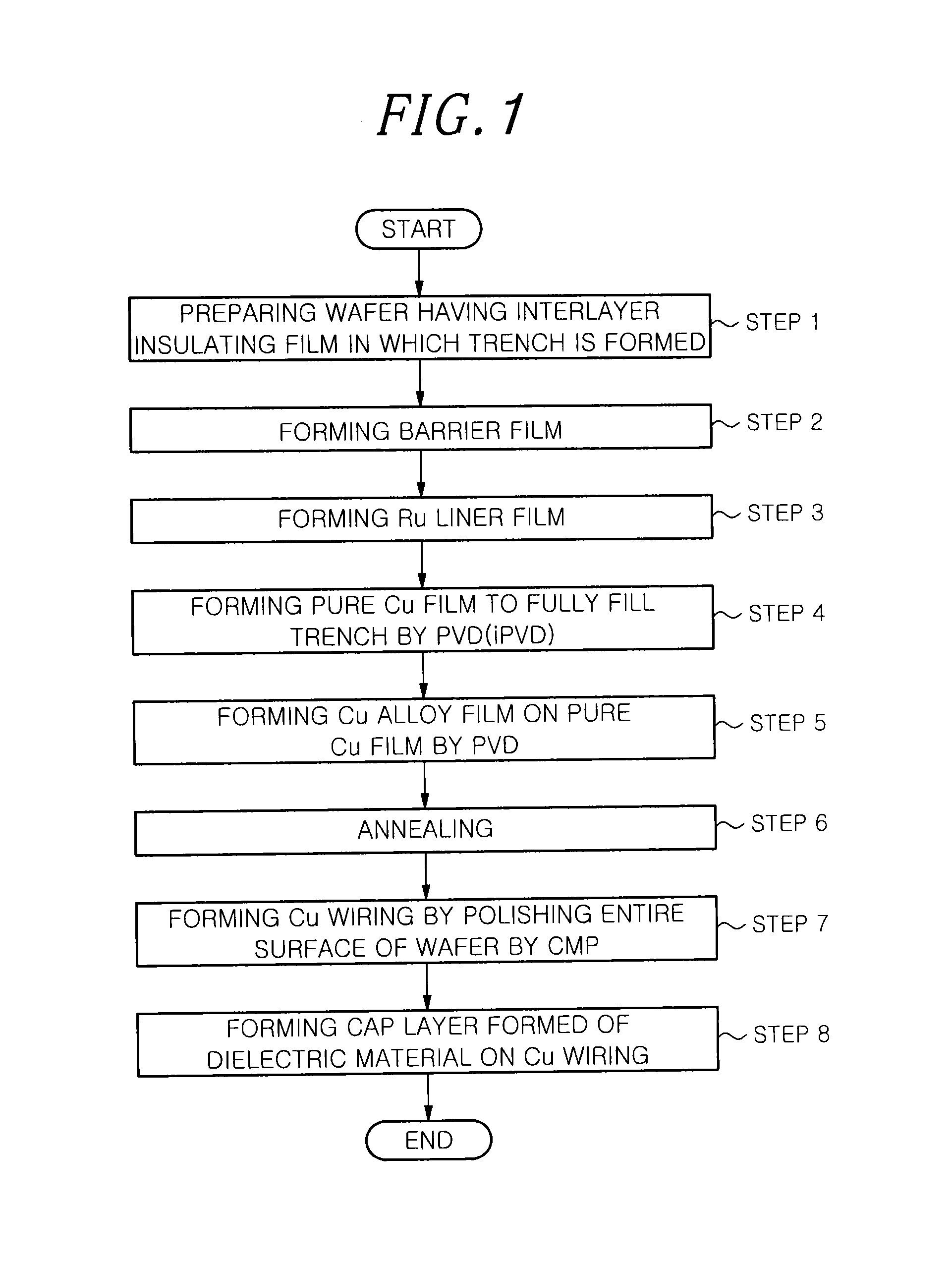
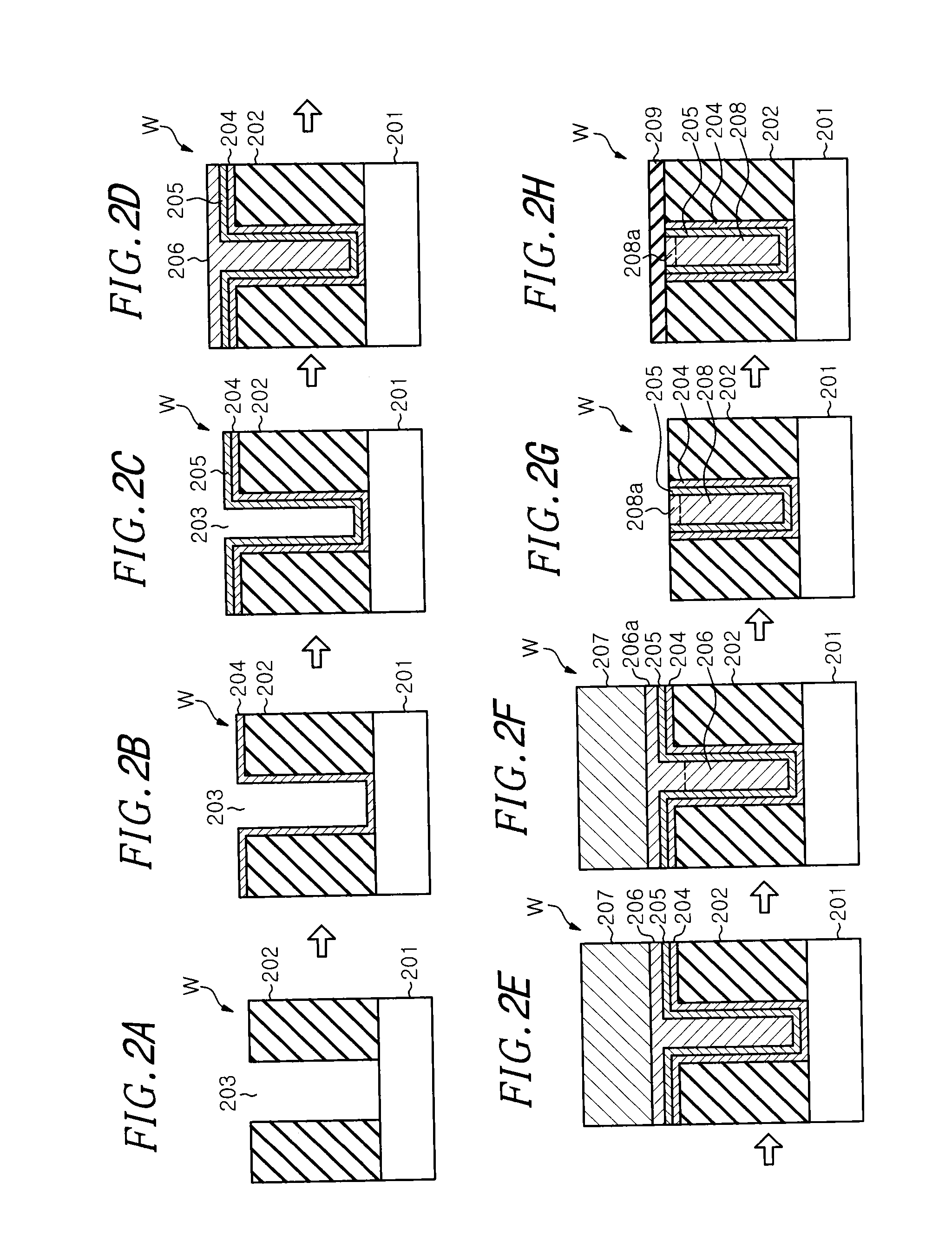
[0033]A Cu wiring forming method in accordance with the present invention will be described with reference to a flowchart shown in FIG. 1 and a process cross sectional view shown in FIGS. 2A to 2H.
[0034]In the present embodiment, first, there is prepared a semiconductor wafer (hereinafter, simply referred to as “wafer”) W including: a base structure 201 (detailed description is omitted); an interlayer insulating film 202 such as a SiO2 film, a Low-k film (SiCO, SiCOH or the like) or the like formed on the base structure 201; and a trench 203 and a via (not shown) for connection with a lower wiring, formed in a predetermined pattern (step 1, FIG. 2A) as a recess. As for the wafer W, it is preferable to remove etching / ashing residue or moisture from a surface of an insulating film by a Degas process or a Pre-Clean process.
[0035]Next, a barrier film 204 for suppressing diffusion of Cu by shielding Cu (acting as a barrier against Cu) is formed on the entire surface including the surface...
second embodiment
[0055]Hereinafter, a Cu wiring forming method in accordance with the present invention will be described with reference to a flowchart shown in FIG. 3 and a process cross sectional view shown in FIGS. 4A to 4H.
[0056]As described in the first embodiment, in the present embodiment, there is provided a wafer W including: a base structure 201 (detailed description is omitted); an interlayer insulating film 202 such as a SiO2 film, a Low-k film (SiCO or SiCOH) or the like formed on the base structure 201; and a trench 203 and a via (not shown) for connection with a lower wiring, formed in a predetermined pattern (step 11, FIG. 4A) as a recess.
[0057]Next, in a same manner as described in the first embodiment, a barrier film 204 for blocking Cu diffusion is formed on the entire surface including the surfaces of the via and the trench 203 (step 12, FIG. 4B). Then, a Ru liner film 205 is formed on the barrier film 204 (step 13, FIG. 4C).
[0058]Thereafter, a pure Cu seed film 210 formed of pur...
third embodiment
[0069]Hereinafter, a Cu wiring forming method in accordance with the present invention will be described with reference to the flowchart shown in FIG. 5 and the process cross sectional views shown in FIGS. 6A to 6H.
[0070]As described in the first and the second embodiment, in the present embodiment, there is prepared a wafer W including: a base structure 201 (detailed description is omitted); an interlayer insulating film 202 such as a SiO2 film, a Low-k film (SiCO, SiCOH or the like) or the like formed on the base structure 201; and a trench 203 and a via (not shown) for connection with a lower wiring, formed in a predetermined pattern (step 21, FIG. 6A) as a recess.
[0071]Next, in a same manner as described in the first and the second embodiment, a barrier film 204 blocking Cu diffusion is formed on the entire surface including the surfaces of the via and the trench 203 (step 22, FIG. 6B). Then, a Ru liner film 205 is formed on the barrier film 204 (step 23, FIG. 6C).
[0072]Next, a ...
PUM
| Property | Measurement | Unit |
|---|---|---|
| thickness | aaaaa | aaaaa |
| thickness | aaaaa | aaaaa |
| thickness | aaaaa | aaaaa |
Abstract
Description
Claims
Application Information
 - Generate Ideas
- Intellectual Property
- Life Sciences
- Materials
- Tech Scout
- Unparalleled Data Quality
- Higher Quality Content
- 60% Fewer Hallucinations
Browse by: Latest US Patents, China's latest patents, Technical Efficacy Thesaurus, Application Domain, Technology Topic, Popular Technical Reports.
© 2025 PatSnap. All rights reserved.Legal|Privacy policy|Modern Slavery Act Transparency Statement|Sitemap|About US| Contact US: help@patsnap.com