Field effect transistor device

a field effect transistor and transistor technology, applied in the field of field effect transistor devices, can solve the problems of unnecessarily complex and expensive associated circuitry, inconvenient use of conventional normally-on hemts, and transistors with not having a uniform threshold voltage, etc., and achieve the effect of high reliability

Active Publication Date: 2014-02-13
NAT CENT UNIV +2
View PDF5 Cites 7 Cited by
  • Summary
  • Abstract
  • Description
  • Claims
  • Application Information

AI Technical Summary

Benefits of technology

[0009]Accordingly, a normally-off field effect transistor device (such as a normally-off heterojunction field effect transistor) with a uniform threshold voltage and a high reliability is provided.

Problems solved by technology

Use of such a negative power supply made the associated circuitry unnecessarily complex and expensive.
The conventional normally-on HEMTs are rather inconvenient to use.
However, creating the recess in the electron supply layer leads to shortcomings wherein the threshold voltage changes substantially with manufacturing errors in the depth of the recess in the electron supply layer, and thus the transistor does not have a uniform threshold voltage and has low reliability due to the poor etching tolerance between the electron supply layer and a layer underlying the electron supply layer.

Method used


Image

  • Field effect transistor device
  • Field effect transistor device
  • Field effect transistor device

Examples


Embodiment Construction

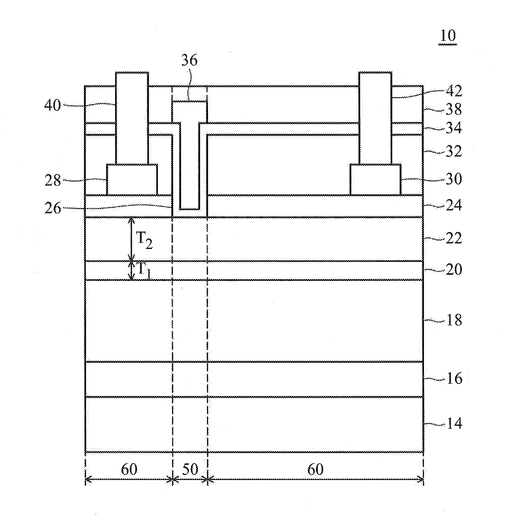
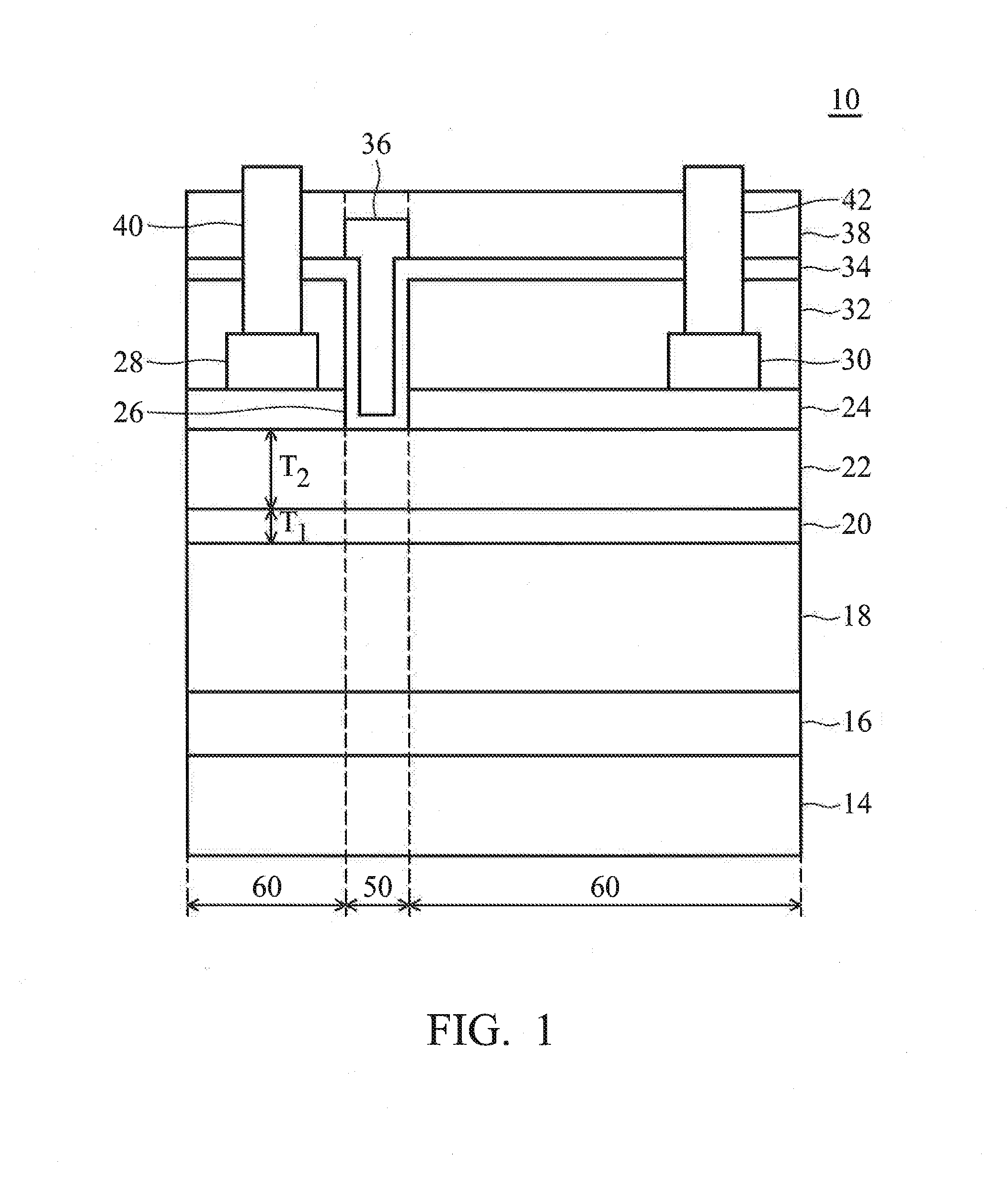
[0021]The following description is of the best-contemplated mode of carrying out the invention. This description is made for the purpose of illustrating the general principles of the invention and should not be taken in a limiting sense. The scope of the invention is best determined by reference to the appended claims.

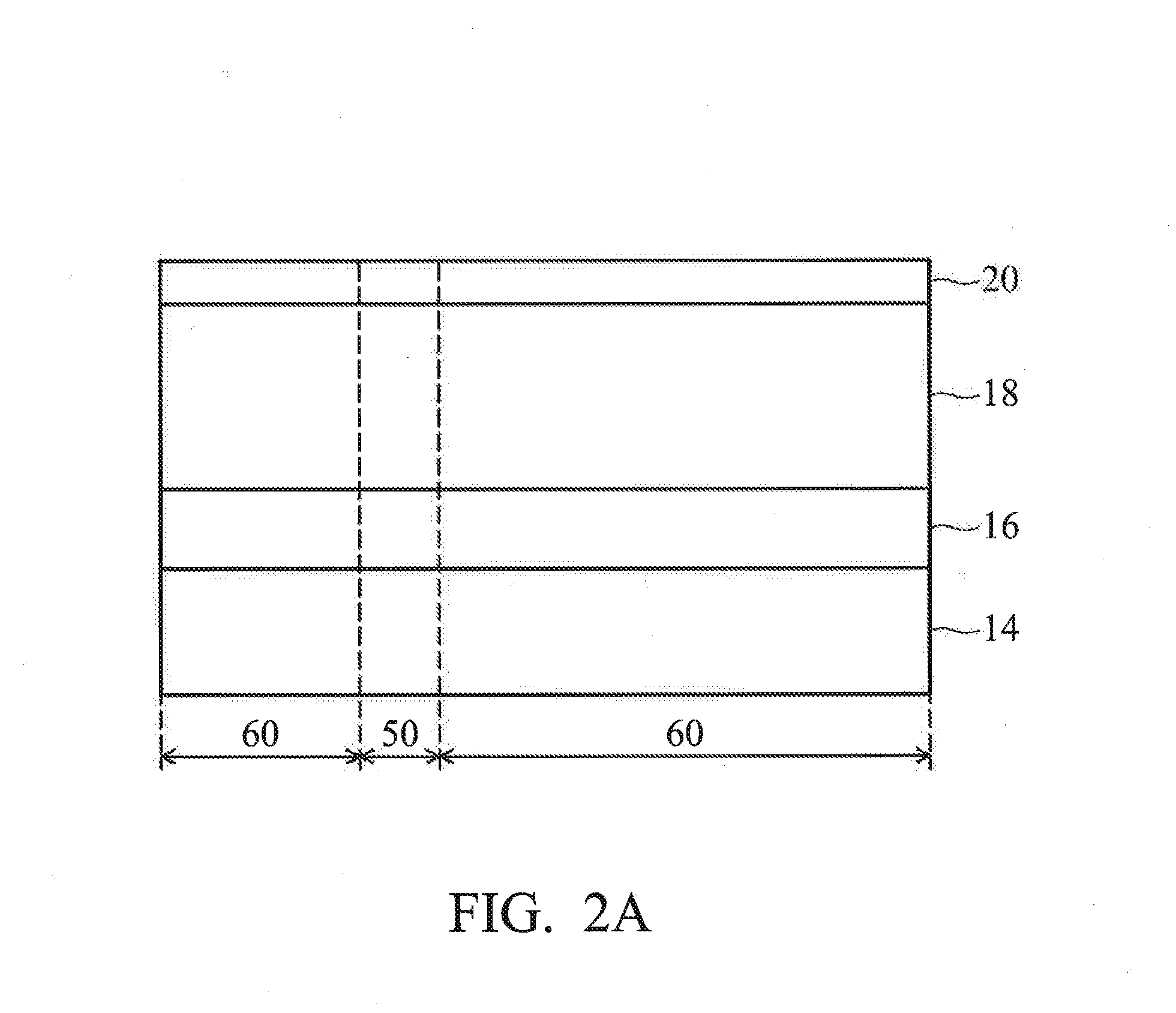
[0022]In FIG. 1, an exemplary field effect transistor device 10 (such as a heterojunction field effect transistor) is illustrated, including a substrate 14. The substrate 14 can be silicon carbide, sapphire; silicon, aluminum nitride, gallium nitride or zinc oxide. Although not shown in the FIG. 1, a transition layer or a nucleation layer can be formed on the substrate to facilitate the growth of semiconductor layers. The nucleation layer is specific to the type of substrate used.

[0023]A buffer layer 16, a channel layer 18, and a first barrier layer 20 are sequentially disposed on the substrate 12. The buffer layer 16 generally provides a more uniform crystal structur...


PUM

PropertyMeasurementUnit
thicknessaaaaaaaaaa
distanceaaaaaaaaaa
thicknessaaaaaaaaaa

Abstract

A field effect transistor device is provided by the invention. The field effect transistor device includes: a substrate; a buffer layer, a channel layer, and a first barrier layer sequentially disposed on the substrate; a two-dimensional electron gas controlling layer disposed on the first barrier layer; a second barrier layer disposed on the two-dimensional electron gas controlling layer, wherein the second barrier layer has a recess passing through the second barrier layer; and a gate electrode filled into the recess and separated from the second barrier layer and the two-dimensional electron gas controlling layer by an insulating layer.

Description

CROSS-REFERENCE TO RELATED APPLICATIONS[0001]This application claims the benefit of U.S. Provisional Application No. 61 / 681,533, filed Aug. 9, 2012, the entirety of which is incorporated by reference herein.BACKGROUND OF THE INVENTION[0002]1. Field of the Invention[0003]The present invention relates to a field effect transistor device, and in particularly to a heterojunction field effect transistor device which is normally-off.[0004]2. Description of the Related Art[0005]A nitride semiconductor has a high electric breakdown field and a high electron saturation velocity. Thus, the nitride semiconductor is expected to be a semiconductor material for semiconductor devices having a high breakdown voltage and a low on-state resistance. Many of the conventional semiconductor devices using the nitride related materials may have heterojunctions. The heterojunction is configured with two types of nitride semiconductors having different bandgap energies from each other and is able to generate...

Claims


Application Information

Patent Timeline
Patent Type & Authority Applications(United States)
IPC IPC(8): H01L29/778H01L29/66
CPCH01L29/66462H01L29/778H01L29/7786H01L29/205H01L29/2003H01L29/517H01L29/4236
Inventor CHYI, JEN-INNLIN, HUI-LINGLEE, GENG-YENCHEN, SHIH-PENG
Owner NAT CENT UNIV
Why Eureka
Try Eureka