Stacked inductor using magnetic sheets, and method for manufacturing same

a technology of inductors and magnetic sheets, applied in the direction of magnets, cores/yokes, magnetic bodies, etc., can solve the problems of inductors having the voltage of their power circuits has decreased, and the inductors have an intrinsic limitation in miniaturization. achieve the effect of high frequency

Active Publication Date: 2014-02-20
COILTRONIX
View PDF2 Cites 4 Cited by
  • Summary
  • Abstract
  • Description
  • Claims
  • Application Information

AI Technical Summary

Benefits of technology

[0025]Unlike conventional power inductors, the present invention can obtain high frequency and high-capacity saturation current. In addition, by using soft magnetic metal powder sheets, the present invention can provide a thin inductor which does not have limitations in width in an economical way, and thus makes it possible to provide a slim laptop computer, cellular phone, display device, etc.BEST MODES FOR CARRYING OUT THE INVENTION
[0026]Hereinafter, the present invention will be described with reference to the drawings.
[0027]FIG. 1 is an exterior view of an embodiment of the present invention. FIG. 1 illustrates an inductor (10) formed by lamination of magnetic sheets, where a terminal (11) is formed at an outermost part thereof. The magnetic sheets are formed by filling up a binder with soft magnetic metal alloy powders.
[0028]As said soft magnetic metal alloy powder, anisotropic or isotropic powder in the form of a flat flake is employed. In addition, as material of the alloy powder, Mo-permalloy, permalloy, Sandust (Fe—Si—Al alloy), Fe—Si alloy, amorphous metal, nano crystal grain, etc. may be used.
[0029]As said binder, EPDM, acrylic resin, polyurethane, silicon rubber, etc., which are applied as organic high molecule matrix material, may be used.
[0030]A terminal is made up of a conductive metal such as Cu. Said terminal is formed by a method according to which a Cu-clad magnetic sheet is selectively etched for only a Cu portion to remain, and nickel and tin may be plated around the copper terminal.

Problems solved by technology

Due to the decrease in the size of semiconductors, the voltage of their power circuits has decreased, and thus even a small change in voltage may lead to malfunction of the devices.
However, such inductors have an intrinsic limitation in miniaturization.
Thus, ferrite-based metal oxides achieve low inductance due to magnetic saturation, and have poor direct current superposition characteristics.
In additon, in the case of an inductor using ferrite, a circuit is placed on a ferrite substrate, and then has to be sintered; in this case, however, the inductor may be distorted during the sintering process, which poses an obstacle in ensuring a certain level of inductance and direct current superposition characteristics.
Thus, such inductors cannot be designed to be wide.
In particular, under the recent circumstances where the size of inductors has been reduced and products with a width of 1 mm or less are manufactured, the width of inductors is much more limited; thus, an inductor using ferrite cannot achieve varous types of inductance, and current superposition characteristcs.
In addition, even in the case of a multilayered inductor using a magnetic sheet filled up with magnetic materials, excellent inductor characteristics could not be achieved simply by including a magnetic sheet in the electrical conductive circuit of the inductor.

Method used


Image

  • Stacked inductor using magnetic sheets, and method for manufacturing same
  • Stacked inductor using magnetic sheets, and method for manufacturing same
  • Stacked inductor using magnetic sheets, and method for manufacturing same

Examples


working example 1

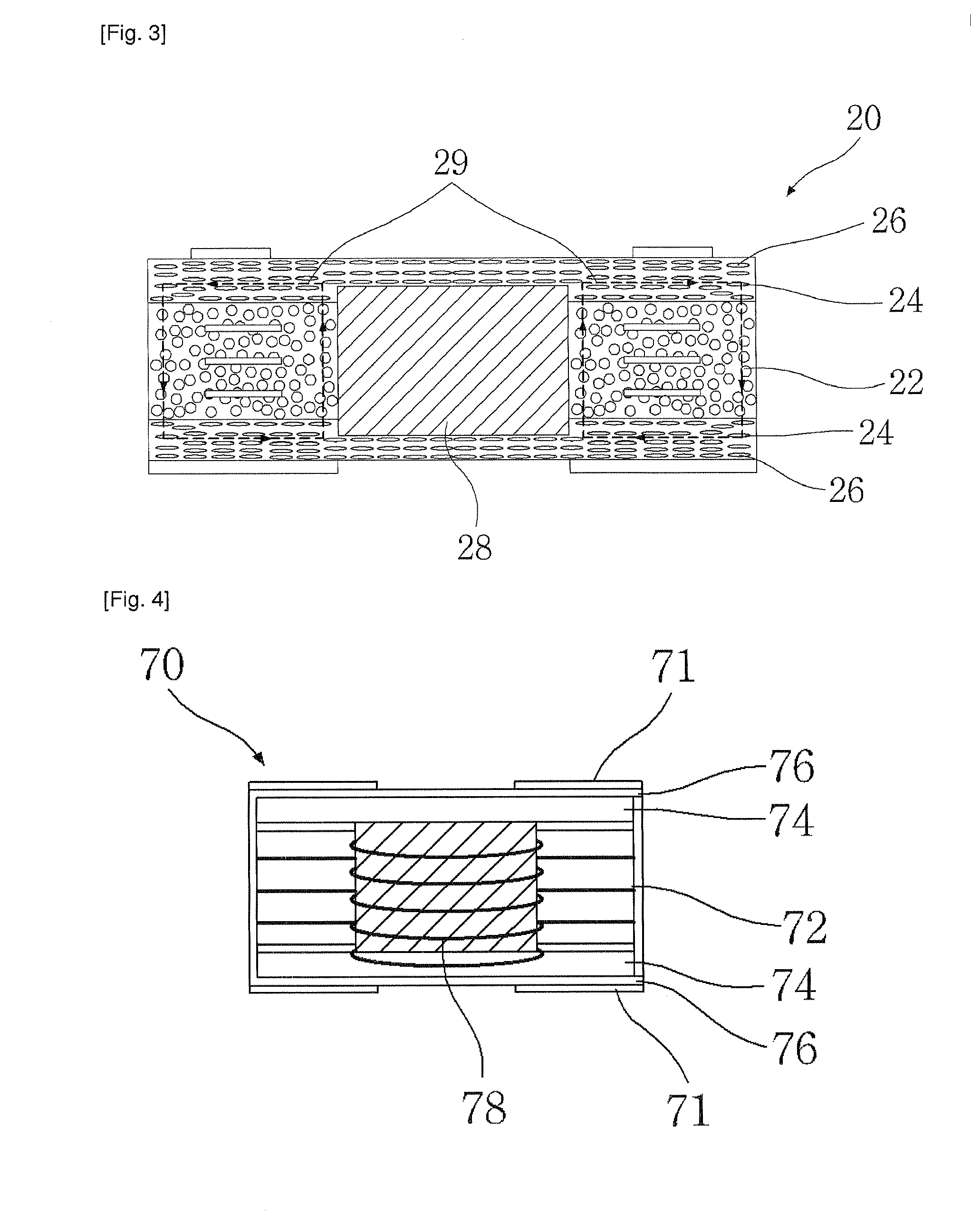
[0051]Three circuit layers were manufactured by etching top and bottom surfaces of a Cu-clad 210×300×0.1 mm magnetic sheet prepared by mixing Fe—Si magnetic powder and EPDM, for 3 minutes with an iron chloride solution at a temperature of 50° C. and forming an electrical conductive circuit.

[0052]A via hole was formed by punching a hole in an electrical circuit by using a drill, with an external diameter of 0.2 mm, of a precise drilling machine, and the inner side of the via hole was plated with Cu.

[0053]Three circuit layers were laminated, a separate Cu clad magnetic sheet is laminated as a land layer onto the upper and lower sides of said circuit layers, and etched to form a land, which is drilled to form a via hole, and the inner side of said via hole was plated with an electrical conductive material.

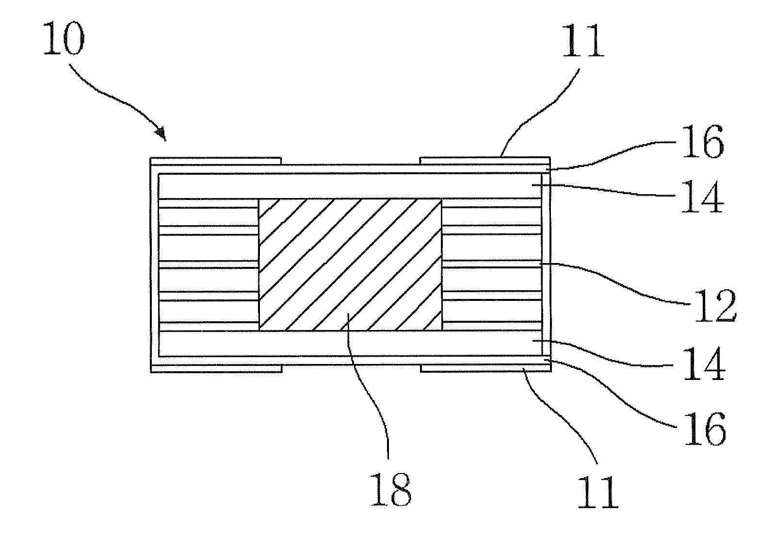
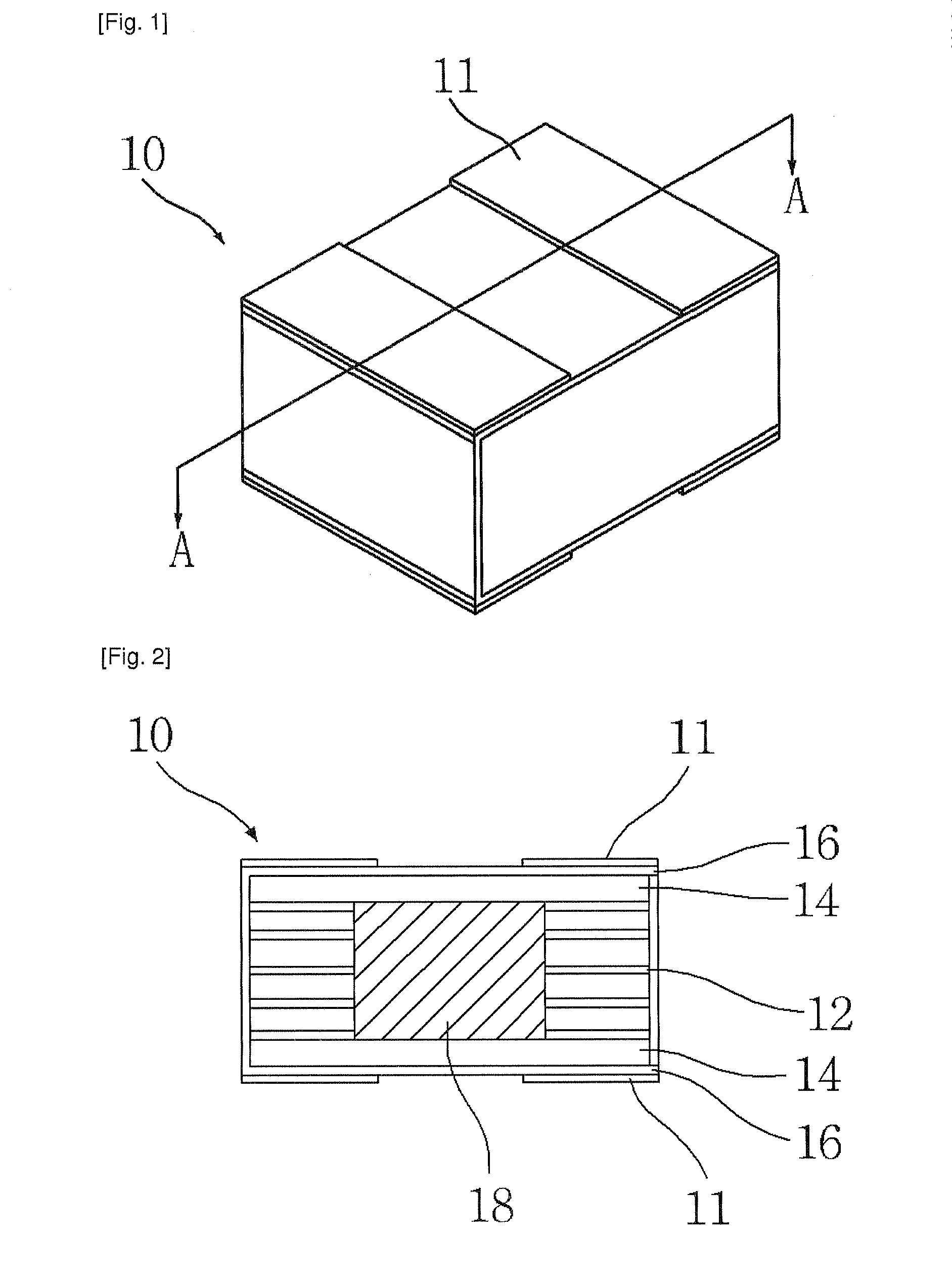
[0054]The circuit layer and the land layer were laminated, and then an inner hollow with the width of 1 mmΦ was formed by punching the inner side, and then a permalloy magnetic core w...

working example 2

[0056]Three 210×300×0.1 mm magnetic sheets prepared by mixing Fe—Si magnetic powder and EPDM were laminated and then the inner side of said magnetic sheets was punched.

[0057]A permalloy magnetic core where a Cu wire of 0.15 mmΦ was wound was inserted into said punched hole of 1 mmΦ. A separate Cu clad magnetic sheet is laminated as a land layer onto the upper and lower sides, and etched to form a land, which is drilled to form a via hole, and the inner side of said via hole was plated with an electrical conductive material.

[0058]Again, a separate Cu clad magnetic sheet is laminated as terminal layer onto the upper and lower sides, and etched to form a terminal, and then drilled to form a via hole, and the inner side of said via hole is plated. Last, surface portions other than said terminal were plated with epoxy.


PUM

PropertyMeasurementUnit
widthaaaaaaaaaa
temperatureaaaaaaaaaa
diameteraaaaaaaaaa

Abstract

The present invention relates to a multilayered chip power inductor with high direct current superposition characteristics and high-frequency characteristics, particularly to a multilayered chip power inductor using as magnetic materials a magnetic sheet filled up with soft magnetic metal powder and a magnetic core. The present invention is to provide a multilayered chip power inductor achieving high inductance and direct current superposition characteristics. In order to achieve the objective, the present invention provides a multilayered chip power inductor using a magnetic sheet, characterized in that a plurality of magnetic sheets are laminated, wherein an electrical conductive circuit is formed on the surfaces of said sheets; that a terminal is formed at an outermost part; that said electrical conductive circuit and said terminal are electrically connected through via holes, and form a circuit in the form of a coil; and that a magnetic core is inserted into said circuit, and a method for manufacturing the same.

Description

DETAILED DESCRIPTION OF THE INVENTION[0001]1. Technical Field[0002]The present invention relates to a multilayered chip power inductor with high direct current superposition characteristics and high-frequency characteristics, particularly to a multilayered chip power inductor using magnetic sheets filled up with soft magnetic metal powder and a magnetic core as magnetic substances.[0003]2. Background Art[0004]Due to the diversification of portable devices, types of the operating power supplies for the power circuit of a portable device have been diversified. For portable devices are used such power supplies as an LCD drive, power amplifier module, base band IC, etc. Each of the power supplies requires a different voltage for operation, and requires a power circuit for converting a voltage supplied from a power source to an operating voltage of its circuit. Due to the decrease in the size of semiconductors, the voltage of their power circuits has decreased, and thus even a small chan...

Claims


Application Information

Patent Timeline
Patent Type & Authority Applications(United States)
IPC IPC(8): H01F41/02
CPCH01F41/02H01F17/0033H01F27/292H01F41/046Y10T29/49078H01F27/00H01F27/245H01F1/14766H01F1/153H01F27/2804H01F27/29H01F2027/2809
Inventor LIM, SUNG TAELEE, TAE KYUNGKIM, DOO INKIM, CHUNG RYUL
Owner COILTRONIX
Why Eureka
Try Eureka