High-voltage microfluidic droplets actuation by low-voltage fabrication technologies

a technology of microfluidic droplets and fabrication technologies, applied in the direction of electrolysis components, separation processes, instruments, etc., can solve the problems of high-voltage cell size, high-voltage cmos fabrication technologies, and excessive joule heating, so as to reduce leakage current, increase high-impedance, and increase breakdown voltage

Inactive Publication Date: 2014-02-27
WANG GARY CHORNG JYH
View PDF2 Cites 21 Cited by
  • Summary
  • Abstract
  • Description
  • Claims
  • Application Information

AI Technical Summary

Benefits of technology

[0020]In some embodiments, the device comprises a CMOS device wherein standard low-voltage (3.5 V-0.4V) CMOS components are used to implement a bi-state-switch. In other embodiments, the device comprises a CMOS device comprising a protection circuitry configured to increase a breakdown voltage, reduce a leakage current of a positive voltage, prevent a short to ground of a negative voltage through p-n junction, increase a high-impedance of bi-state-switc

Problems solved by technology

However, excessive Joule heating is a problem for DEP actuation, even though it can be reduced by using materials of higher thermal conductivity or by reducing structure size.
High-voltage CMOS fabrication technologies has several issues.
The first issue is the size of the high-voltage cells.
Moreover, power consumption, stability/cost of the fabrication technologies and compatib

Method used


Image

  • High-voltage microfluidic droplets actuation by low-voltage fabrication technologies
  • High-voltage microfluidic droplets actuation by low-voltage fabrication technologies
  • High-voltage microfluidic droplets actuation by low-voltage fabrication technologies

Examples


Embodiment Construction

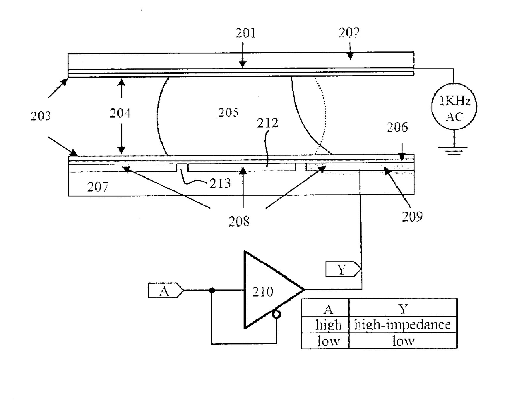
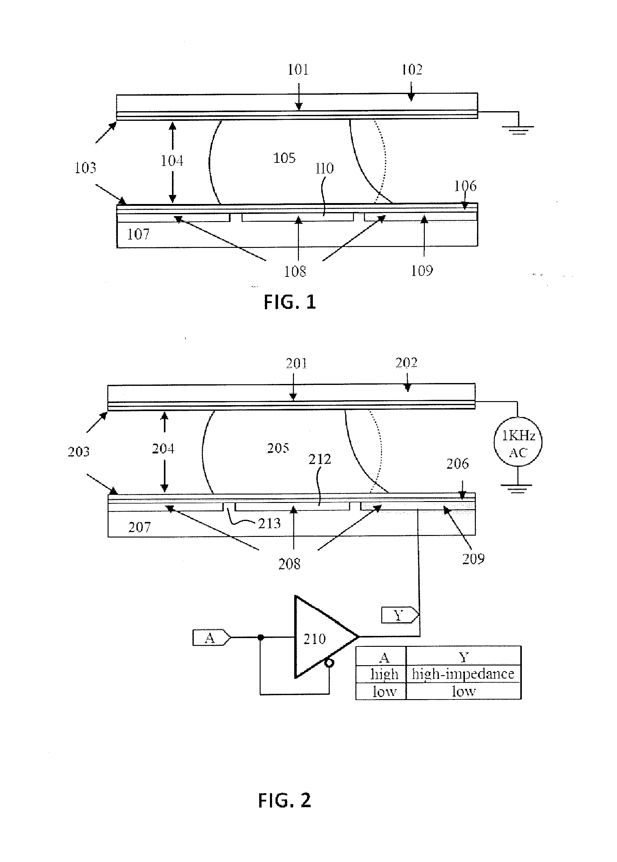
[0026]A conventional electrowetting microactuator mechanism is illustrated in FIG. 1. The digital microfluidic device comprises two parallel plates 102 and 107, respectively, with a distance gap 104. The bottom plate 107 contains an array of individually controllable electrodes 108, and the top plate 102 is coated with a continuous ground electrode 101. Electrodes are able to be formed by a material, such as indium tin oxide (ITO) that has the combined features of electrical conductivity and optical transparency in thin layer. A dielectric insulator 106, e.g., parylene C, coated with a hydrophobic film 103 such as Teflon AF, is added to the plates to decrease the wettability of the surface and to add capacitance between the droplet and the control electrode. The droplet 105 containing biochemical samples and the filler medium, such as the silicone oil or air, are sandwiched between the plates to facilitate the transportation of the droplet 105 inside the filler medium. In order to m...


PUM


Abstract

A bi-state-switch low-voltage fabrication technique is able to be used to construct microfluidic systems leveraging well-established low-voltage semiconductor fabrication technologies to achieve high-voltage droplet actuation applications with lower costs, smaller device sizes, and also less time. Also, the electrode cells are able to be made using the well-established low-voltage CMOS fabrication technologies, which can be used to make large-scale integrated microelectronics and microfluidics.

Description

FIELD OF THE INVENTION[0001]The present invention relates to the actuation of microfluidic droplets, which is considered as high-voltage applications from semiconductor fabrication point of view by using standard low-voltage semiconductor fabrication technologies.[0002]The present invention is able to be used to advance the construction of future digital microfluidic systems with large-scale microelectronic and microfluidic integration because the present invention enables the standard semiconductor fabrication technologies to implement digital microfluidic systems.BACKGROUND OF THE INVENTION[0003]In droplet-based microfluidic devices, a liquid is sandwiched between two parallel plates and transported in the form of droplets. Droplet-based microfluidic systems offer many advantages: low power consumption and require no mechanical components such as pumps or valves. In recent years, droplet-based microfluidic systems have been broadly utilized in applications such as the mixing of an...

Claims


Application Information

Patent Timeline
IPC IPC(8): B03C5/02
CPCB03C5/02
Inventor WANG, GARY CHORNG-JYH
Owner WANG GARY CHORNG JYH
Why Eureka
Try Eureka