
Composite Substrates, Light Emitting Devices and a Method of Producing Composite Substrates

a technology of composite substrates and light emitting devices, which is applied in the direction of polycrystalline material growth, crystal growth process, chemically reactive gas, etc., can solve the problems of cracks or fractures in the gan layer of the gan template, and achieve the effect of small warping amoun

Inactive Publication Date: 2014-02-27
NGK INSULATORS LTD
View PDF3 Cites 9 Cited by
  • Summary
  • Abstract
  • Description
  • Claims
  • Application Information

AI Technical Summary

Benefits of technology

The present invention is about a way to make a composite substrate by growing a layer of gallium nitride crystal on a sapphire body. The goal is to reduce thermal stress between the gallium nitride crystal and sapphire body, which helps to create a composite substrate with less warping. This approach can help to create better quality semiconductor devices using these composite substrates.

Problems solved by technology

During this trial, however, cracks or fractures were generated in the GaN layer of the GaN template at a high temperature (>1000° C.
), which was problematic.

Method used


Image

  • Composite Substrates, Light Emitting Devices and a Method of Producing Composite Substrates
  • Composite Substrates, Light Emitting Devices and a Method of Producing Composite Substrates
  • Composite Substrates, Light Emitting Devices and a Method of Producing Composite Substrates

Examples


example 1

Processing of Sapphire Body

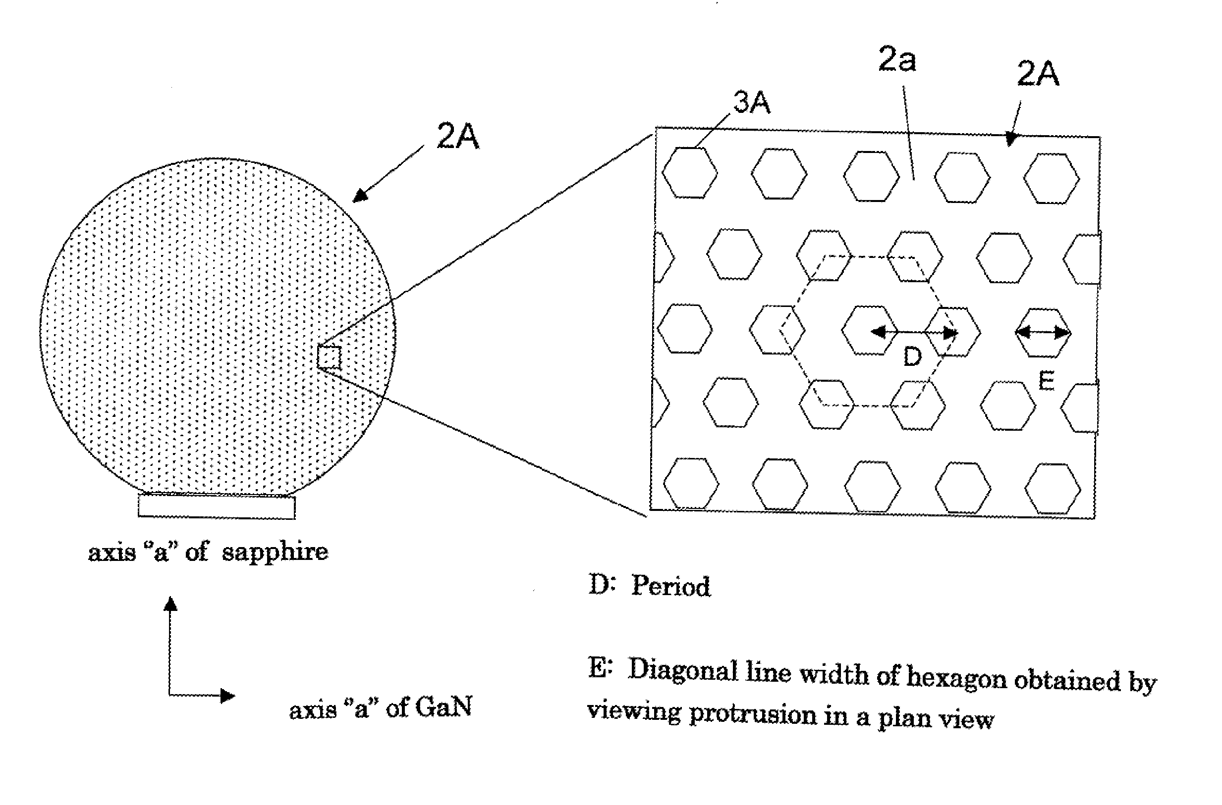
[0069]A resist having a thickness of 1 μm was patterned on a surface of a c-face sapphire body having a diameter of 2 inches and a thickness of 500 μm using photolithography. As to the resist pattern, the pattern was designed so that the hexagonal prisms, each having a diagonal line width “E” of 4 μm, were arranged at a period “D” of 6 μm so as to be six-fold rotational symmetrical. This was subjected to etching for 10 minutes using a chlorine-based dry etching system to etch the sapphire body to a depth of about 1.5 μm where it is not covered by the resist, to leave protrusions each having a shape of hexagonal prism where the resist was present. The residue of the resist was removed by a remover.

[0070]It was thereby obtained a sapphire body 2A as shown in FIG. 6. That is, a plurality of protrusions 3A were formed on a c-face 2a of the sapphire body 2A. Each of the protrusions 3A has a shape of a hexagonal prism, and the protrusions 3A were positioned so a...

example 2

[0088]A c-face sapphire body having a diameter of 2 inches was etched by applying chlorine based dry etching in a depth of about 2 μm according to the same procedure as the Example 1, except that a thickness of the resist was made 0.5 μm, so that the shape of each protrusion was proved to be six-sided pyramid.

[0089]The sapphire body after the processing of the protrusions and recesses was used to form the underlying layer according to the same procedure as the Example 1. The warping was about 20 μm, and it was observed spaces, each having a size of 1 μm to several μm, between the protrusions. Thereafter, a GaN composite substrate was produced and films for an LED structure were then formed, according to the same procedure as the Example 1.

[0090]The substrate was taken out of the MOCVD furnace and then observed by eyes to prove that cracks were not observed. Further, it was observed by a differential interference contrast microscope to prove that the surface was flat.

[0091]The wafer ...

example 3

[0092]A c-face sapphire body having a diameter of 2 inches was etched by applying chlorine based dry etching in a depth of about 2 μm according to the same procedure as the Example 1, except that the period of the protrusions “D” was made 6 μm and the diagonal line width “E” of the hexagon was made 3 μm, so that the shape of each protrusion was proved to be hexagonal prism.

[0093]The sapphire body after the processing of the protrusions and recesses was used to form the underlying layer according to the same procedure as the Example 1. The warping was about 25 μm, and it was observed spaces, each having a size of 1 μm to several μm, between the protrusions. Thereafter, a GaN composite substrate was produced and films for an LED structure were then formed, according to the same procedure as the Example 1.

[0094]The substrate was taken out of the MOCVD furnace and then observed by eyes to prove that cracks were not observed. Further, it was observed by a differential interference contra...


PUM

PropertyMeasurementUnit
thicknessaaaaaaaaaa
widthaaaaaaaaaa
widthaaaaaaaaaa

Abstract

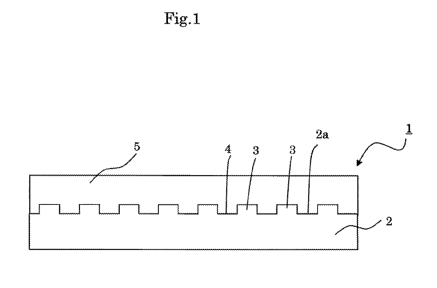
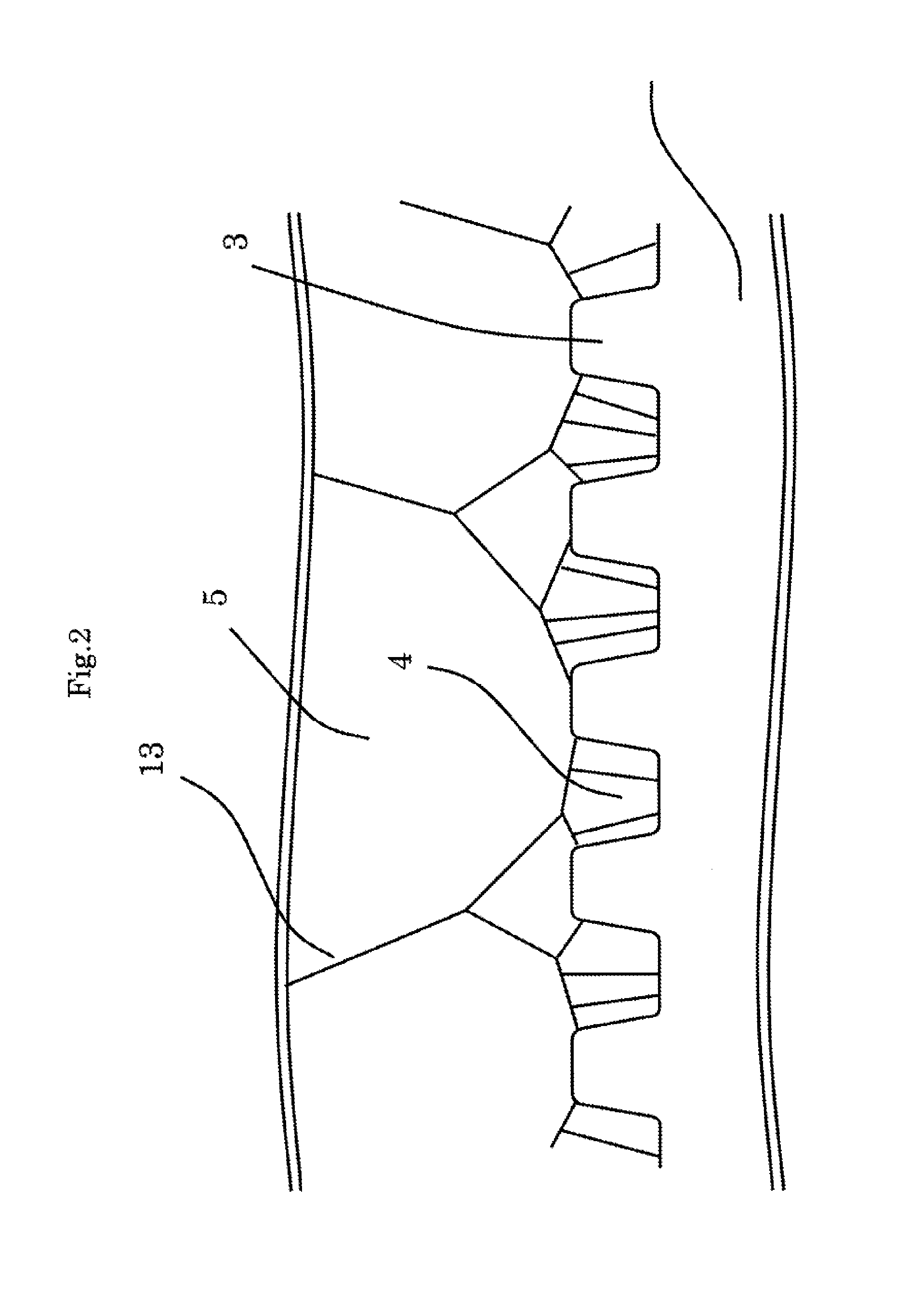
A plurality of protrusions 3 are provided on a c-face 2a of a sapphire body 2. An underlying layer 5 made of gallium nitride is then grown by vapor phase epitaxy process on the c-face 2a. A gallium nitride crystal layer 6 is then provided by flux method on the underlying layer 5. Each of the protrusions 3 has a shape of a hexagonal prism or a six-sided pyramid. Differences of growth rates of the gallium nitride crystal around the protrusions 3 are utilized to relax a stress between the sapphire body and gallium nitride crystal and to reduce cracks or fractures due to the stress.

Description

FIELD OF THE INVENTION[0001]The present invention relates to a composite substrate including a sapphire body and gallium nitride crystal grown thereon, a light emitting device and a method of producing a composite substrate.RELATED ART STATEMENTS[0002]It is described a method of growing gallium nitride crystal on a sapphire body in Japanese Patent Publication Nos. 2000-021772A and 2001-168028A, for example.SUMMARY OF THE INVENTION[0003]A seed crystal substrate is produced by forming GaN layer by MOCVD or the like on a c-face sapphire body with a flat surface and then used to grow GaN layer thereon by flux method at a growth temperature of 800 to 900° C. in a thickness of 10 to 100 μm, so that it can be produced a GaN template including the GaN layer with a low dislocation density and providing the uppermost surface.[0004]The inventors have tried to produce an LED structure by MOCVD using this GaN template. During this trial, however, cracks or fractures were generated in the GaN lay...

Claims


Application Information

Patent Timeline
Patent Type & Authority Applications(United States)
IPC IPC(8): H01L33/00H01L21/02H01L33/22H01L33/32H01L29/06H01L29/20
CPCH01L33/007H01L29/0657H01L29/2003H01L21/0254H01L33/32H01L21/0242H01L21/0243H01L33/22C30B25/186C30B29/406H01L21/02458H01L21/02639H01L21/0265H01L33/02H01L33/16H01L33/20
Inventor IWAI, MAKOTOKURAOKA, YOSHITAKA
Owner NGK INSULATORS LTD
Learn More