
Patterned nanoparticle structures

a nanoparticle and nanoparticle technology, applied in the direction of non-metal conductors, sustainable manufacturing/processing, instruments, etc., can solve the problems of limited materials involved in the use of these techniques, limited material types, and limited to large micron scale dimensions

Active Publication Date: 2014-03-13
UNIV OF MASSACHUSETTS
View PDF14 Cites 54 Cited by
  • Summary
  • Abstract
  • Description
  • Claims
  • Application Information

AI Technical Summary

Benefits of technology

This patent describes how to create patterned structures using nanoparticles. The nanoparticles can be manipulated using electromagnetic radiation and a patterned mold or mask, resulting in the creation of very small patterns. These patterns can be formed in a layered fashion to create a three-dimensional structure. The technical effects of this invention include the ability to create highly precise, patterned structures using nanoparticles, which could be useful in various applications such as electronics, sensors, and biomedical devices.

Problems solved by technology

The types of materials that are involved using these techniques are limited.
Further, such subtractive processes can be expensive and wasteful.
This technique, however, has a number of disadvantages by being slow, limited to large micron scale dimensions, unable to be used to manipulate semi-crystalline, crystalline or conducting compositions at low temperature, and is not easily scalable.

Method used


Image

  • Patterned nanoparticle structures
  • Patterned nanoparticle structures
  • Patterned nanoparticle structures

Examples


example 1

Solvent Exchange of Metal Oxide Nanoparticles

[0104]A 250 mL beaker was charged with 100 g of the specific acidic or basic metal oxide nanoparticle dispersion or mixed metal oxide nanoparticle dispersion and 50 g each of NMP and MeOH was added. The solvent was then evaporated until most of the residual water was removed. Once the water was removed the solids remaining were diluted to the desired concentration with a 50:50 mixture of NMP and MeOH. The system was subjected to ultra-sonication for 5 minutes to completely re-disperse the nanoparticles into the organic solvents, while maintaining the solution at room temperature with a recirculating water bath. The dispersion after sonication was translucent.

example 2

High Refractive Index Planar TiO2 Hard Coat

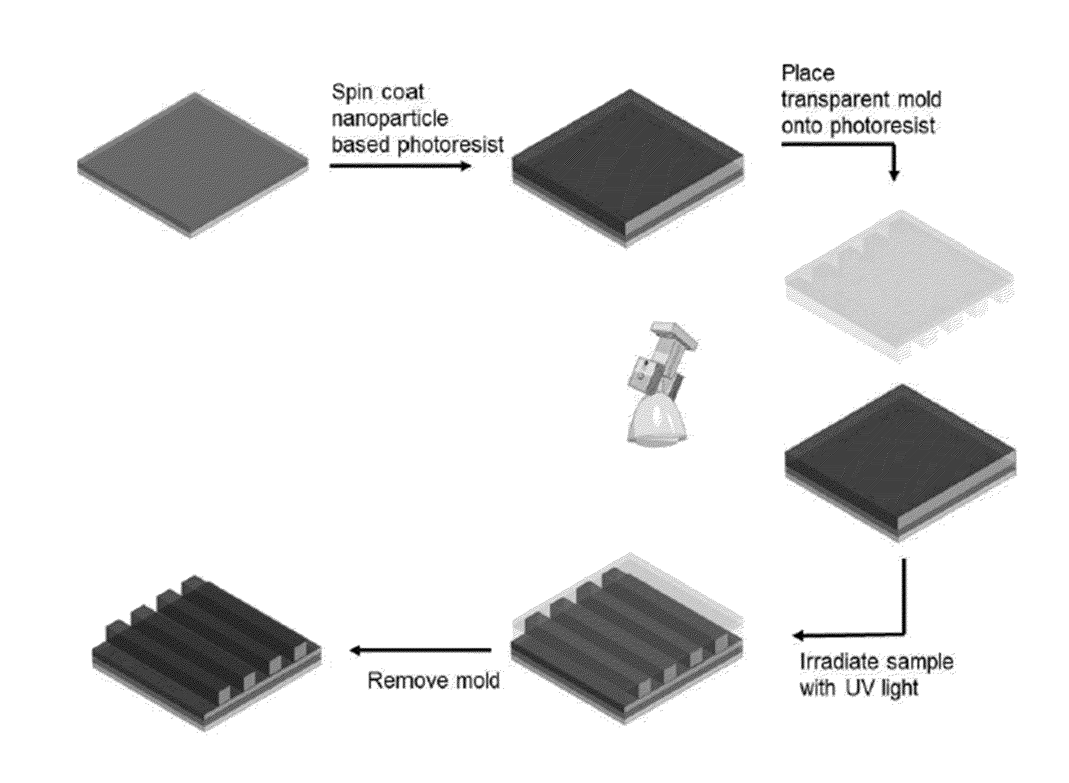
[0105]Solvent exchanged titanium dioxide nanoparticles using the procedure from Example 1 (13.2 wt % TiO2 in a 50:50 mixture of NMP:MeOH) was added to a 20 mL glass vial along with a 13.2 wt % solution of NOA60 in NMP in amounts varying from 0 wt % NOA60 to 90 wt % NOA60. The amount of NOA60 that was added was adjusted to obtain the desired refractive index. FIG. 20 illustrates the refractive index versus wavelength of planar patterned nanoparticle nanostructures based on TiO2 (5 nm to 30 nm in particle size) and a commercially available thiol-ene based photoresist (NOA60). The solution was filtered through a 0.2 micron PTFE filter and then spun coat on a substrate (silicon, glass, or plastic, depending on the application) in a low humidity environment at 3000 rpm until no solvent remained (approximately 2 minutes). The coating was then irradiated with 365 nm UV light for 15 min with an intensity of 12 mW / cm2 under a nitrogen environment.

[0...

example 3

Patterned TiO2 Nanoparticle Nanocomposites Using Organic Solvent Dispersible Formulations

[0109]Solvent exchanged titanium dioxide nanoparticles using the procedure in Example 1 (13.2 wt % TiO2 in a 50:50 mixture of NMP:MeOH) was added to a 20 mL glass vial along with a 13.2 wt % solution of NOA60 in NMP in amounts varying from 0 wt % NOA60 to 90 wt % NOA60. The amount of NOA60 was adjusted to obtain the desired refractive index, as can be seen in FIG. 20. The solution was filtered through a 0.2 micron PTFE filter and then spun coat on a substrate (silicon, glass, or plastic, depending on the application) in a low humidity environment at 3000 rpm for 30 seconds and then the mold was placed on top of the substrate with the coating. The coating was then irradiated with 365 nm UV light for 15 min with an intensity of 12 mW / cm2 under a nitrogen environment. The mold was carefully peeled off of the coating and the characteristic diffraction pattern for the particular mold could be seen ov...


PUM

PropertyMeasurementUnit
particle sizeaaaaaaaaaa
thicknessaaaaaaaaaa
widthaaaaaaaaaa

Abstract

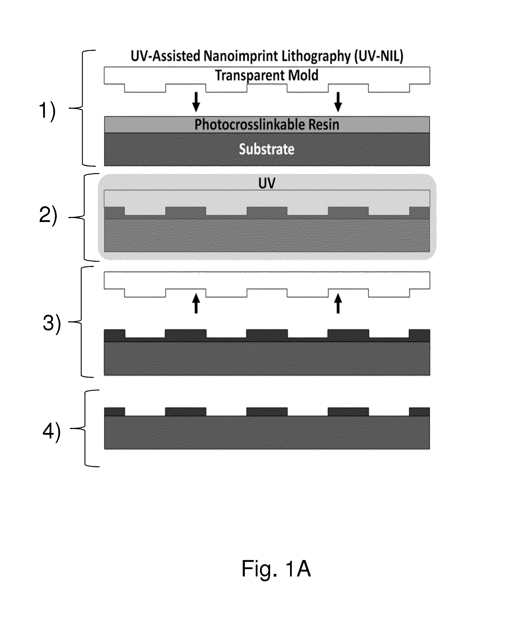
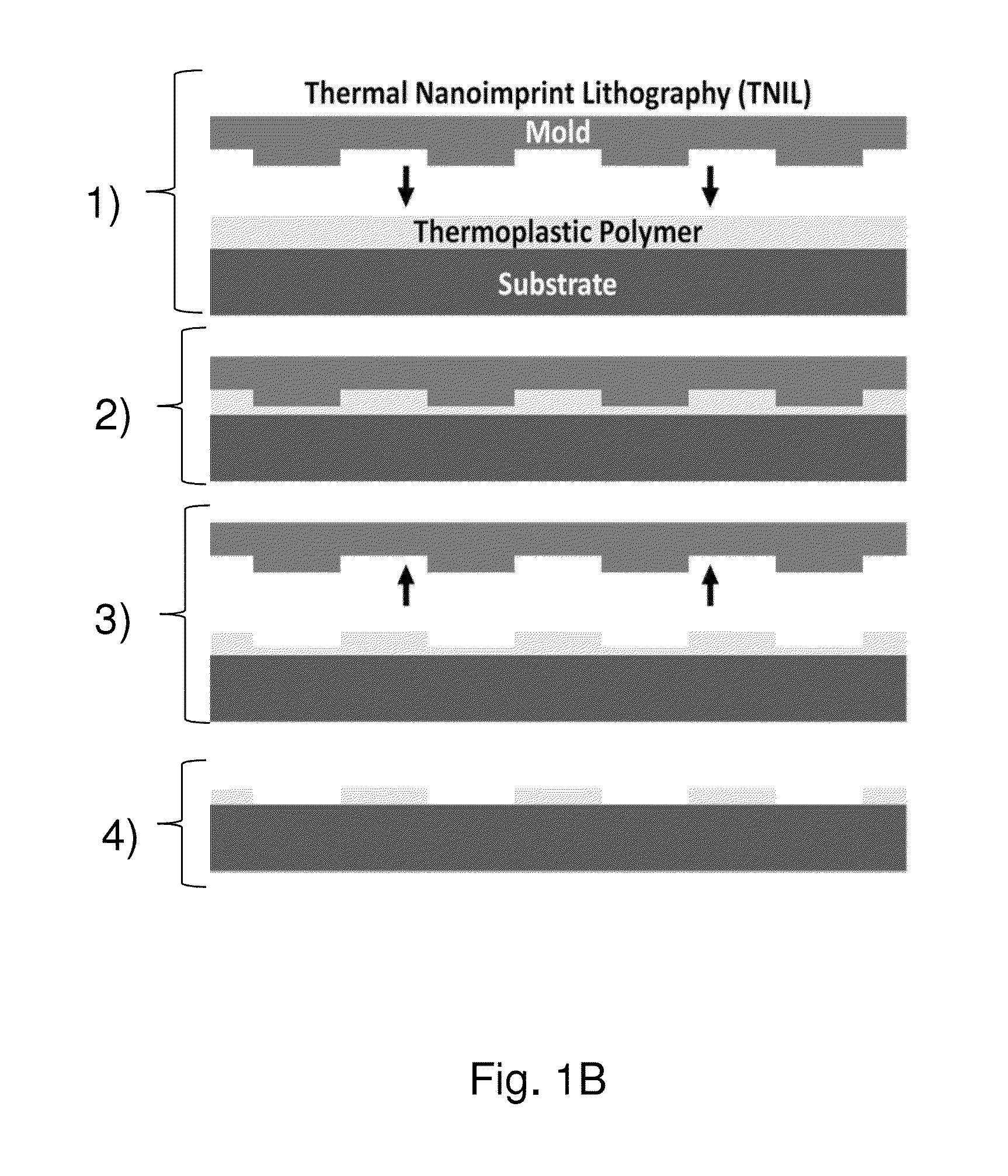
Aspects relate to patterned nanostructures having a feature size not including film thickness of below 5 microns. The patterned nanostructures are made up of nanoparticles having an average particle size of less than 100 nm. A nanoparticle composition, which, in some cases, includes a binder material, is applied to a substrate. A patterned mold used in concert with electromagnetic radiation function to manipulate the nanoparticle composition in forming the patterned nanostructure. In some embodiments, the patterned mold nanoimprints a suitable pattern on to the nanoparticle composition and the composition is cured through UV or thermal energy. Three-dimensional patterned nanostructures may be formed. A number of patterned nanostructure layers may be prepared and suitably joined together. In some cases, a patterned nanostructure may be formed as a layer that is releasable from the substrate upon which it is initially formed. Such releasable layers may, in turn, be arranged to form a three-dimensional patterned nanostructure in accordance with suitable applications.

Description

FEDERALLY SPONSORED RESEARCH[0001]Research leading to various aspects of embodiments presented herein were sponsored, at least in part, by the National Science Foundation, Grant No. CMMI-1025020. The United States Government may have certain rights in the invention.FIELD OF INVENTION[0002]Aspects described herein relate generally to patterned nanostructures comprising nanoparticles.BACKGROUND[0003]Devices having improved optical and electronic properties have gained increasing interest, particularly at the sub-micron length scale. Such devices may be composed of inorganic materials such as metals, metal oxides, semiconductors (e.g., silicon), carbonaceous or other amorphous, crystalline and / or semi-crystalline compositions. Traditional manufacturing techniques for semiconductors having certain opto-electronic properties involve subtractive processes where material is built up and removed through various mask / etch processes. The types of materials that are involved using these techni...

Claims


Application Information

Patent Timeline
Patent Type & Authority Applications(United States)
IPC IPC(8): H01B1/08H01B13/00H01B3/10H10K99/00
CPCH01B1/08H01B13/003H01B3/10B82Y30/00H01M4/04H01M8/124H01M8/1286H01M6/40Y02P70/50Y02E60/50H10K71/211H10K30/82H10K50/813H10K2102/331H01M4/0433Y10T428/24893G02B1/118
Inventor WATKINS, JAMESBEAULIEU, MICHAEL R.HENDRICKS, NICHOLAS R.
Owner UNIV OF MASSACHUSETTS
Learn More