
Hierarchical Carbon Nano and Micro Structures

a technology of carbon nano and microstructure, which is applied in the direction of yarn, transportation and packaging, synthetic resin layered products, etc., can solve the problems of not facilitating the fabrication of high aspect ratio structures obtaining anisotropic properties, the existing fabrication methods of pyrolysed nanowires are not compatible with standard microfabrication techniques, and the inability to manufacture nanowires

Active Publication Date: 2014-03-20
INTERUNIVERSITAIR MICRO ELECTRONICS CENT (IMEC VZW) +1
View PDF7 Cites 49 Cited by
  • Summary
  • Abstract
  • Description
  • Claims
  • Application Information

AI Technical Summary

Benefits of technology

The present disclosure provides a method for manufacturing carbon micro- or nanostructures by using a polymeric material that is subjected to a plasma etching process to form polymeric nanostructures, which are then pyrolyzed to form pyrolyzed carbon nanostructures. This method allows for the fabrication of pyrolyzed carbon nanostructures with a limited number of steps and can be used for various applications such as electrical integration. The method may also include steps of patterning the polymeric material and depositing a polymeric material onto a substrate. The compounds that can mask the plasma etching process can be metallic, ceramic, or other micro or nanoparticles present in the polymeric material or co-deposited during the plasma etching process.

Problems solved by technology

While this process is interesting for fabricating mats of randomly oriented nanowires, it does not facilitate the fabrication of high aspect ratio structures obtaining anisotropic properties.
Further most of the existing fabrication methods for pyrolysed nanowires are not compatible with standard microfabrication techniques.
While this process enables nanoscale roughening the surface, it does not permit the fabrication of nanowires (i.e. nanoscale solid rods made out of amorphous carbon).
This process leads to the formation of carbon nanotubes (a SP2 hybridized carbon lattice) and does not permit the formation of amorphous nanowires.

Method used


Image

  • Hierarchical Carbon Nano and Micro Structures
  • Hierarchical Carbon Nano and Micro Structures
  • Hierarchical Carbon Nano and Micro Structures

Examples


example

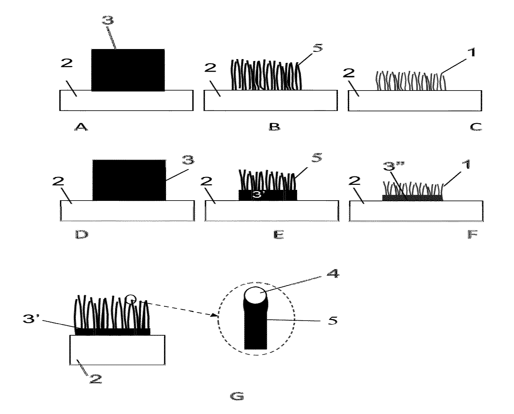
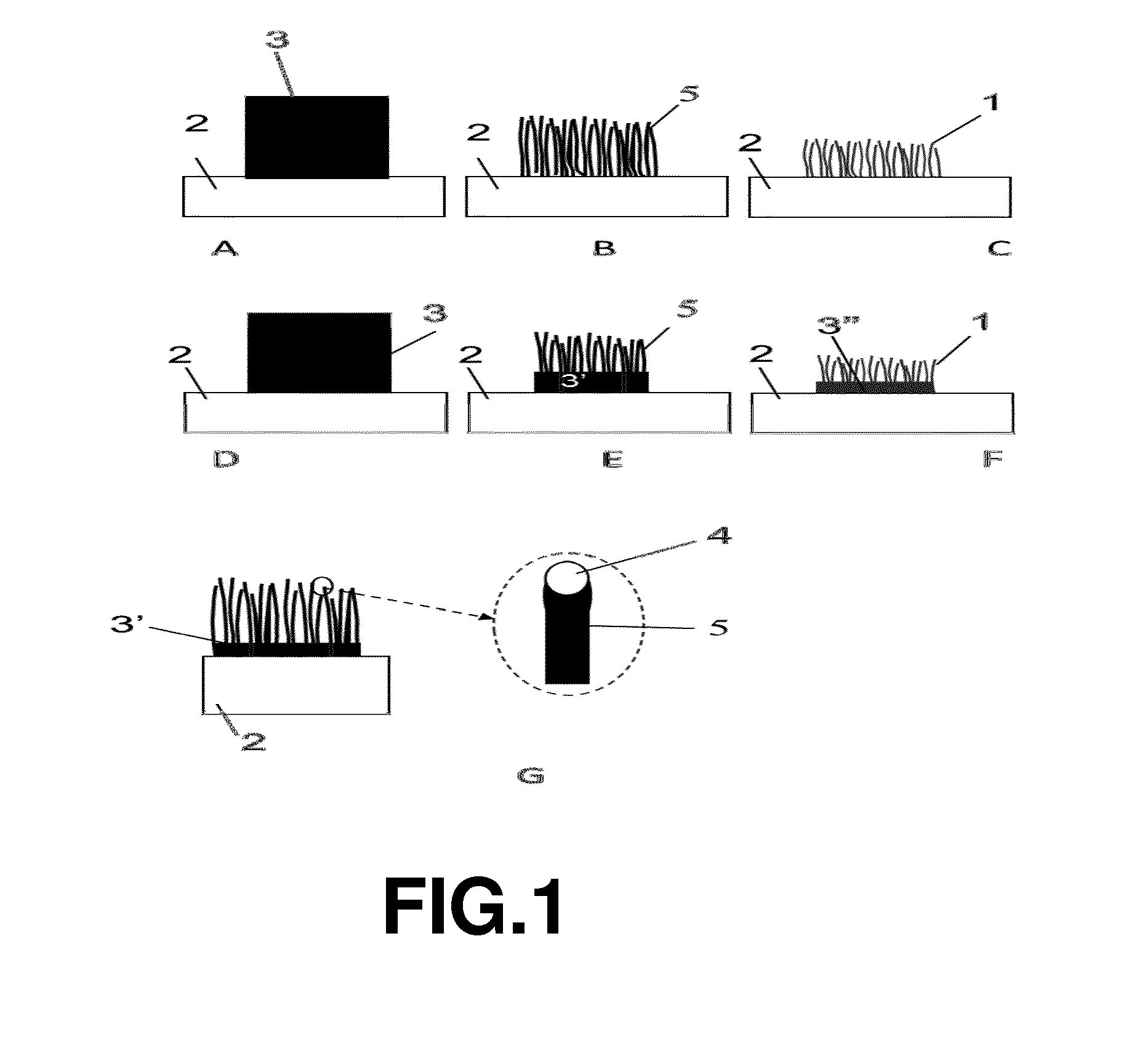
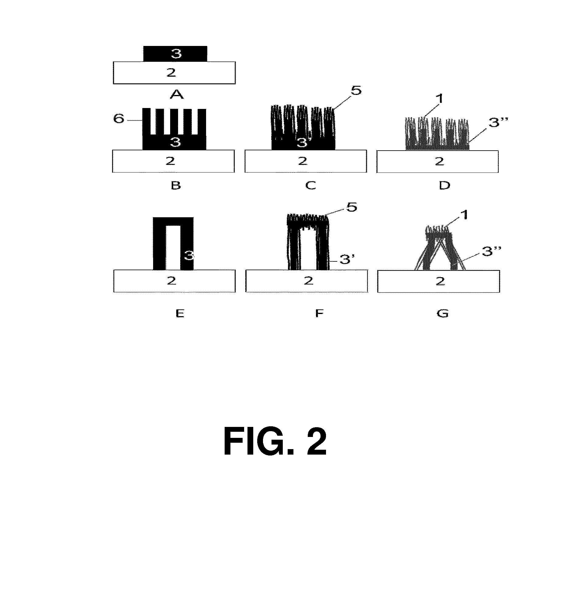
[0198]The CNW fabrication process began by the patterning of su-8® microstructures by standard UV photolithography (FIG. 3A top). Su-8 is a negative photoresist that is commonly used to fabricate high aspect ratio microstructures, and does not reflow during pyrolysis. Next, the sample was exposed to a harsh O2 plasma treatment (5-60 min, 300 w, 200 sccm O2, 150 mtorr in an 8″ tempress ml 200 plasma etcher), which establishes the anisotropic nanowire texture of the su-8 (see FIG. 3A middle). Without behind bond by theory, we believe different mechanisms enabling the formation of su8 nanowires are possible. First, su8® photoresist contains antimony, which is accumulated at the surface upon plasma etching, and can reach up to 19% of the surface composition of our samples after plasma treatment as observed through xps (x-ray photoelectron spectroscopy) analysis (see table 1). Antimony, together with small amounts of aluminum that are sputtered from the plasma chamber can locally mask th...


PUM

PropertyMeasurementUnit
Lengthaaaaaaaaaa
Lengthaaaaaaaaaa
Lengthaaaaaaaaaa

Abstract

Disclosed are methods for fabricating pyrolysed carbon nanostructures. An example method includes providing a substrate, depositing a polymeric material, subjecting the polymeric material to a plasma etching process to form polymeric nanostructures, and pyrolysing the polymeric nanostructures to form carbon nanostructures. The polymeric material comprises either compounds with different plasma etch rates or compounds that can mask a plasma etching process. The plasma etching process may be an oxygen plasma etching process.

Description

FIELD OF THE DISCLOSURE[0001]The present disclosure relates to fabrication methods for pyrolysed carbon nanostructures, the obtained products and devices herewith and its related applications.BACKGROUND OF THE DISCLOSURE[0002]Nanostructured carbon emerged as one of the most promising nano materials of the last decades. Ranging from graphene sheets to fullerenes, nanotubes (CNTs) and diamond like coatings, various types of carbon structures have been developed, each with their own fascinating properties. Besides these well known allotropes, various other interesting types of carbon materials exist that are typically fabricated by pyrolysis of an organic polymer.[0003]Amorphous carbon may be particularly interesting in applications requiring a wide electrochemical stability window, excellent bio-compatibility, and good thermal conductivity.[0004]For these reasons, as well as its cost-effective fabrication, G. Whitesides, M. Madou and others [Schueller, O. J. A., Brittain, S. T. & Whit...

Claims


Application Information

Patent Timeline
IPC IPC(8): C01B31/02C01B31/00
CPCC01B31/00C01B31/0206B81C1/00031B82Y30/00B82Y40/00C01B32/00C01B32/15C01B32/16C01B32/18Y10T428/2481Y10T428/2918
Inventor DE VOLDER, MICHAEL
Owner INTERUNIVERSITAIR MICRO ELECTRONICS CENT (IMEC VZW)
Learn More