Electrical connecting element having nano-twinned copper, method of fabricating the same, and electrical connecting structure comprising the same

Active Publication Date: 2014-04-03
NAT CHIAO TUNG UNIV
View PDF1 Cites 21 Cited by
  • Summary
  • Abstract
  • Description
  • Claims
  • Application Information

AI Technical Summary

Benefits of technology

[0035]The electrical connecting structure having nano-twinned copper of the present invention comprises the above-mentioned electrical connecting element having nano-twinned copper. As a result of this, since the nano-twinned copper layer structure contains a rich content of vacancy sinks, which can absorb and scatter the vacancy concentration diffusing to the interface due to copper-tin reaction, to make vacancies

Problems solved by technology

The electrical connecting process requires high temperature reflow soldering, as a result a reaction between copper metal and solder would form intermetallic compounds (IMCs), as well as voids that are detrimental to the operation of the elements.
Upon the number and volume of the voids are increased to a certain level, the mechani

Method used


Image

  • Electrical connecting element having nano-twinned copper, method of fabricating the same, and electrical connecting structure comprising the same
  • Electrical connecting element having nano-twinned copper, method of fabricating the same, and electrical connecting structure comprising the same
  • Electrical connecting element having nano-twinned copper, method of fabricating the same, and electrical connecting structure comprising the same

Examples


embodiment 1

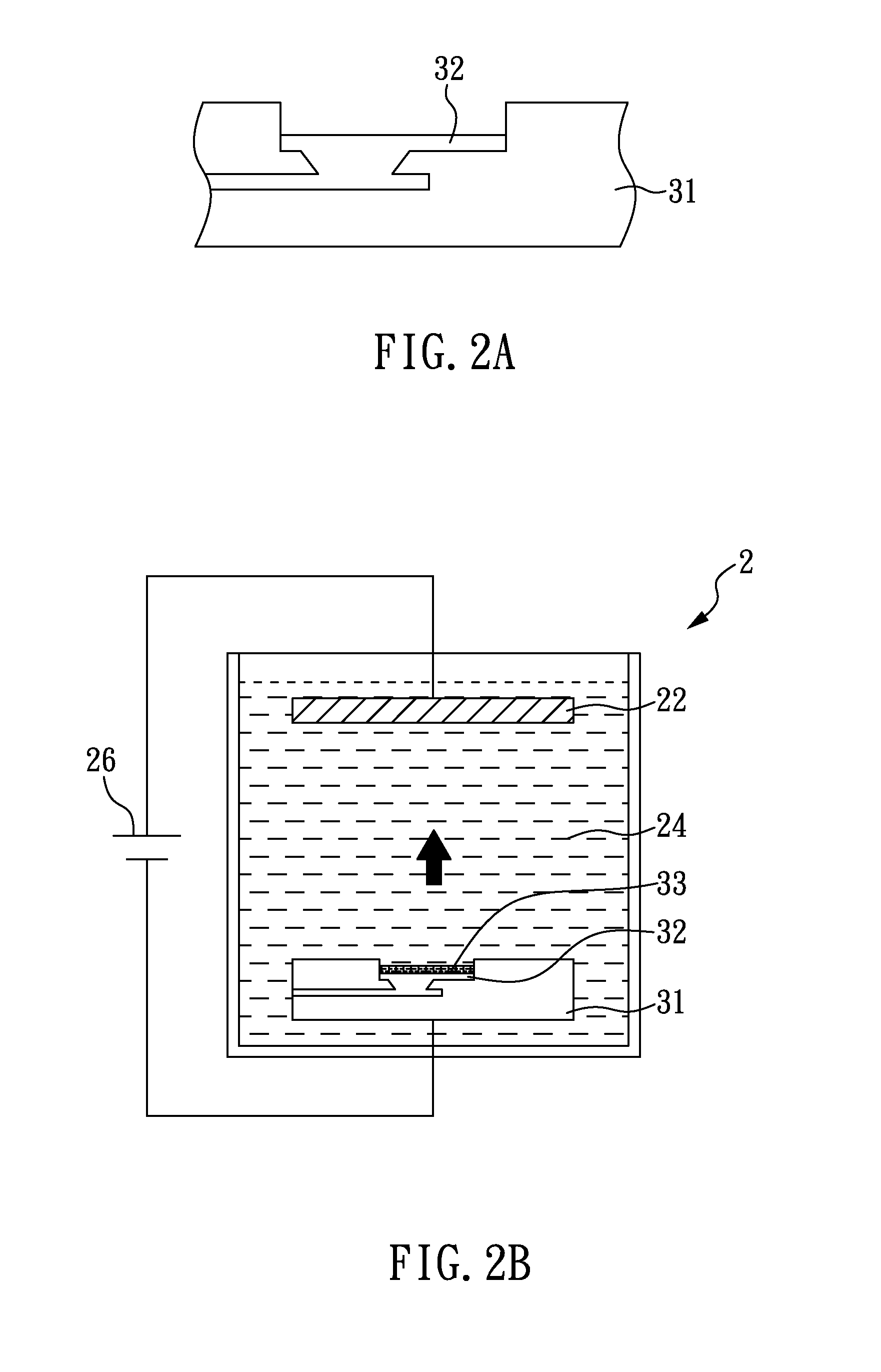
[0058]FIGS. 2A to 2D show the flowcharts for the preparation of the electrical connecting element of the current embodiment. As shown in FIG. 2A, the preparation begins with providing a substrate 31, wherein, the substrate 31 is a printed circuit board having a wiring layer 32 (which can also be used as an electrical pad). Next, which is shown in FIG, 2B, is to place the substrate 31 into an electroplating device 2 to be used as a cathode. The electroplating device 2 comprises an anode 22, which is immersed in the electroplating solution 24 and is connected to a direct current power supply source 26 (for which Keithley 2400 is used in this case). The material used in the anode 22 is metal copper, phosphor bronze or inert anode (e.g. platinum coated titanium). The electroplating solution 24 comprises copper sulfate (copper ion concentration being 20-60 g / L), chloride ion (whose concentration being 10-100 ppm), and methanesulfonic acid (whose concentration being 80-120 g / L), and other...

embodiment 2

[0066]In the current embodiment, as shown in FIG. 3A, a nano-twinned copper layer 43 (used as an electrical pad) is grown on the surface of two semiconductor chips 41 by way of the same electroplating methods described for Embodiment 1.

[0067]Then, a solder is used (not shown in the Figures, the solder of the current embodiment is pure tin, thickness of which is 10 μm) to bind the two semiconductor chips 41 by reflowing at 260° C. for 0.05. hours. It is then followed by another reflow at 260° C. for 1 hour, so as to make the solder transform into an intermetallic compound layer having Cu3Sn layers 44 and a Cu6Sn5 layer 45 with direction-less atomic ordering. Herein, the Cu3Sn layer 44 has a thickness of 1 μm, and the thickness of the Cu6Sn5 layer 45 is 9 μm. After reflow is complete, all solders (not shown in Figures) are transformed into intermetallic compound layer 47. As shown in FIG. 3A, the structure of the intermetallic compound layer 47 is a three-layered structure comprising ...

embodiment 3

[0070]In reference to FIG. 4A, the electrical connecting structure 4 having nano-twined copper for the current embodiment is for the most part equivalent to the electrical connecting structure of Embodiment 2, except for the difference where the thickness of the solder 46 of the current Embodiment is larger, and only a portion of the solder 46 is transformed into the intermetallic compound layer 47 after a reflow process.

[0071]FIG. 4B shows a cross-sectional FIB image of the electrical connecting element 49 of the current embodiment. In this embodiment, the electrical connecting element having nano-twinned copper comprises (reference is also drawn to FIG. 4A): two nano-twinned copper layers 43; an intermetallic compound layer 47, which is disposed between the two nano-twinned copper layers 43 and comprises Cu3Sn layers 44 and Cu6Sn5 layers 45; a solder 46, which is disposed between two Cu6Sn5 layers 45. Therefore, the electrical connecting element 49 of the current embodiment has a ...


PUM

PropertyMeasurementUnit
Temperatureaaaaaaaaaa
Angleaaaaaaaaaa

Abstract

An electrical connecting element, a method of fabricating the same, and an electrical connecting structure comprising the same are disclosed. The method of fabricating the electrical connecting structure having twinned copper of the present invention comprises steps of: (A) providing a first substrate; (B) forming a nano-twinned copper layer on part of a surface of the first substrate; (C) forming a solder on the nano-twinned copper layer of the first substrate; and (D) reflowing the nano-twinned Cu layer and solder to produce a solder joint, wherein at least part of the solder reacts with the nano-twinned copper layer to produce an intermetallic compound (IMC) layer which comprises a Cu3Sn layer, This invention reduces the voids formation in the interface between the intermetallic compound and the solder, and then enhances the reliability of solder joints.

Description

CROSS-REFERENCE TO RELATED APPLICATIONS[0001]This application is a continuation-in-part of U.S. application Ser. No. 13 / 829,256 filed Mar. 14, 2013, which is incorporated by reference. This application also claims the benefits of the Taiwan Patent Application Serial Number 101136825 filed on Oct. 5, 2012 and the Taiwan Patent Application Serial Number 101143398 filed on Nov. 21, 2012, the subject matters of which are incorporated herein by reference.FIELD OF INVENTION[0002]The present invention relates to a preparation method for making an electrical connecting structure having nano-twinned copper, an electrical connecting element having nano-twinned copper, and an electrical connecting structure having nano-twinned copper, particularly to a preparation method for making an electrical connecting structure having nano-twinned copper which can reduce kirkendall voids generated from copper-tin reactions, an electrical connecting element having nano-twinned copper, and an electrically c...

Claims


Application Information

Patent Timeline
IPC IPC(8): H05K1/09H05K3/40
CPCH05K3/40H05K1/09H01L2224/81948H01L21/4846H01L24/03H01L24/05H01L24/11H01L24/13H01L24/16H01L24/81H01L2224/03462H01L2224/05541H01L2224/05571H01L2224/05647H01L2224/11849H01L2224/13022H01L2224/13083H01L2224/13111H01L2224/13147H01L2224/81191H01L2224/81447H01L2224/8181H01L2224/81815H01L2924/3651H01L2224/16503H01L23/49811H01L23/49866H01L2224/16145H01L2224/16237H01L2924/00014H01L2924/3656H01L2224/0401H01L2924/01322H01L2924/15787H01L2924/00011Y10T29/49149Y10T29/49155H01L2924/0105H01L2924/00012H01L2224/05552H01L2924/00H01L2224/81805
Inventor CHEN, CHIHCHIU, WEI-LAN
Owner NAT CHIAO TUNG UNIV
Why Eureka
Try Eureka