Semiconductor device manufacturing method

a manufacturing method and semiconductor technology, applied in semiconductor devices, semiconductor/solid-state device details, electrical apparatus, etc., can solve the problems of inability to carry out patterning positioning, low atmospheric pressure, increase in frequency of maintenance, etc., to prevent auto-doping, prevent breakdown, and prevent the breakdown of alignment mark form

Inactive Publication Date: 2014-04-17
FUJI ELECTRIC CO LTD
View PDF7 Cites 13 Cited by
  • Summary
  • Abstract
  • Description
  • Claims
  • Application Information

AI Technical Summary

Benefits of technology

[0012]In this way, there is a trade-off relationship between preventing auto-doping and preventing a breakdown in alignment mark form. As it is possible to prevent both auto-doping and a breakdown in alignment mark form when carrying out epitaxial growth in a low pressure atmosphere (for example, 20 Torr) using multilayer epitaxial technology, there is no trade-off relationship. However, epitaxial growth rate in a low pressure atmosphere is such that atmospheric pressure is low compared with epitaxial growth in an atmospheric pressure (in the region of, for example, 760 Torr), and the frequency of maintenance increases due to sediment on the chamber side walls and discharge pipe, and so on, because of which there is a problem in that productivity deteriorates.
[0013]The invention, in order to eliminate the heretofore described problems with the heretofore known technology, provides a semiconductor device manufacturing method such that it is possible to improve the trade-off relationship between auto-doping and breakdown in alignment mark form. The invention, in order to eliminate the heretofore described problems with the heretofore known technology, provides a semiconductor device manufacturing method with high productivity.
[0025]According to the invention, it is possible to prevent auto-doping by epitaxial layers being grown on the main surface of an arsenic doped substrate at atmospheric pressure, with the epitaxial growth temperature at 1,150° C. to 1,180° C., and the epitaxial growth rate at 2.2 μm per minute to 2.6 μm per minute. Also, according to the invention, it is possible to prevent a breakdown in the form of an alignment mark newly formed in an epitaxial layer grown on the main surface of an arsenic doped substrate in which an alignment mark is formed. Also, according to the invention, it being possible to prevent breakdown in alignment mark form means that it is possible to reduce the number of times an additional step for forming an alignment mark is carried out compared with that heretofore known.
[0026]According to the semiconductor device manufacturing method according to the invention, an advantage is achieved in that it is possible to improve the trade-off relationship between auto-doping and breakdown in alignment mark form. According to the semiconductor device manufacturing method according to the invention, an advantage is achieved in that it is possible to improve productivity.

Problems solved by technology

Because of this, an exposure device is unable to recognize the alignment mark when patterning during selective ion implantation for selectively forming a p-type region in an n-type epitaxial layer, and a problem occurs in that it is not possible to carry out patterning positioning (alignment).
However, epitaxial growth rate in a low pressure atmosphere is such that atmospheric pressure is low compared with epitaxial growth in an atmospheric pressure (in the region of, for example, 760 Torr), and the frequency of maintenance increases due to sediment on the chamber side walls and discharge pipe, and so on, because of which there is a problem in that productivity deteriorates.

Method used


Image

  • Semiconductor device manufacturing method
  • Semiconductor device manufacturing method
  • Semiconductor device manufacturing method

Examples


embodiment

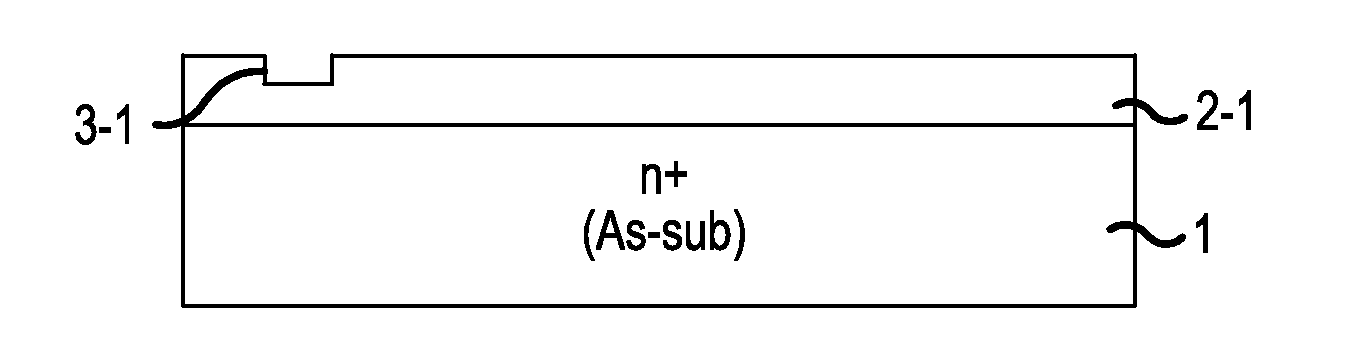
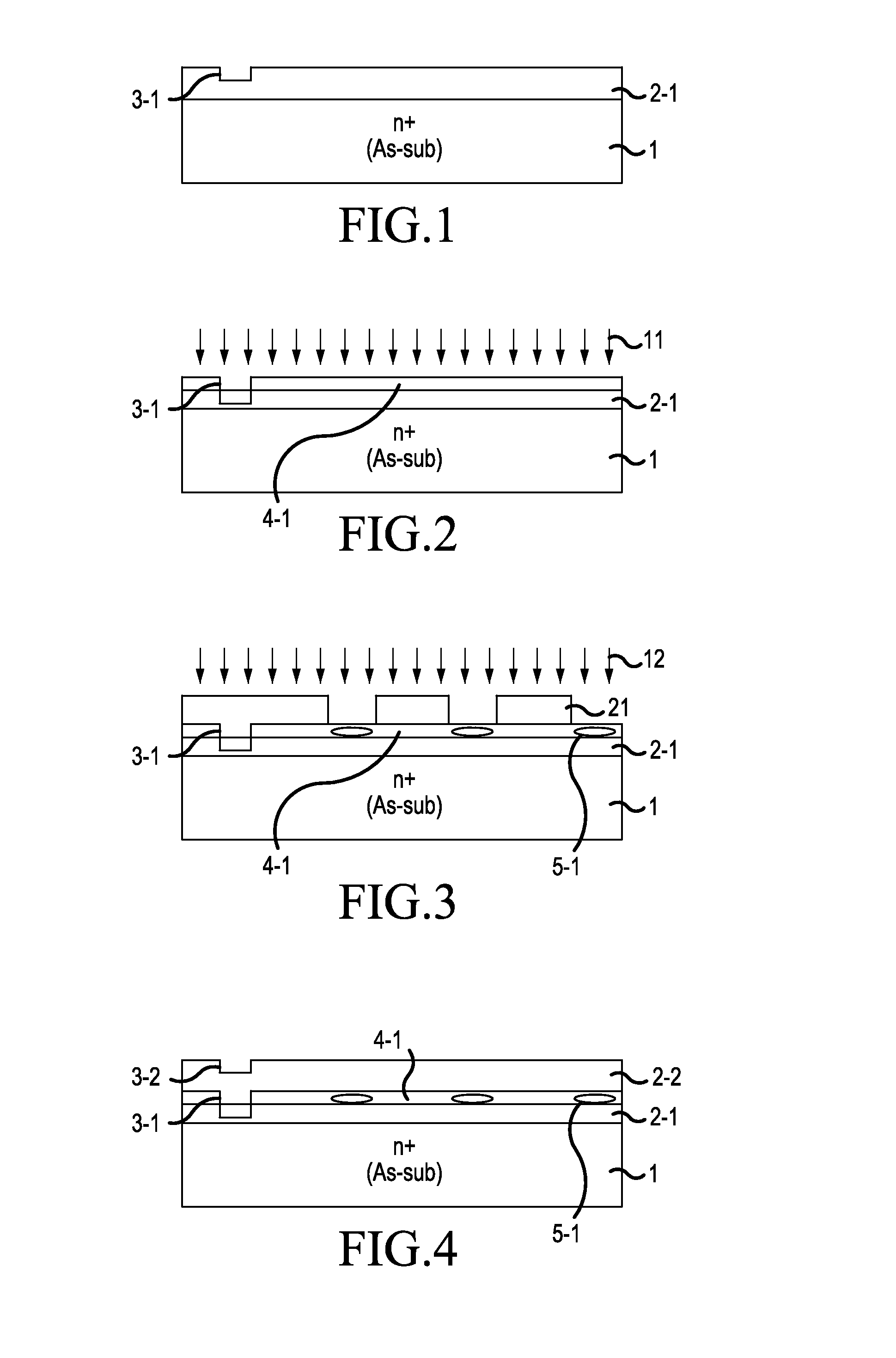
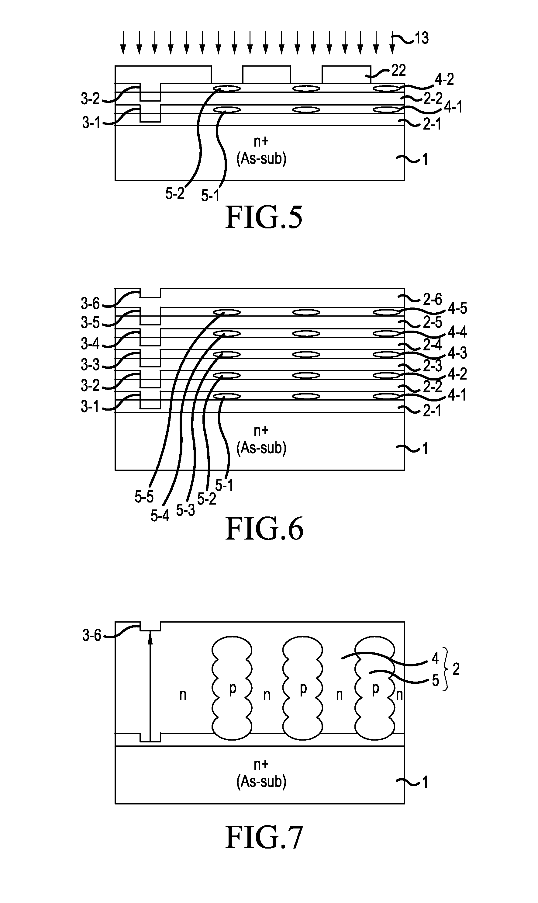
[0046]A description will be given of the semiconductor device manufacturing method according to the embodiment, with a case of fabricating a super junction MOSFET as an example. FIGS. 1 to 7 are sectional views showing conditions partway through the manufacture of a semiconductor device according to the embodiment. Firstly, arsenic (As) doped low resistance n+ type silicon substrate (an arsenic doped substrate) 1 is prepared, as shown in FIG. 1. Arsenic doped substrate 1 has a resistivity of, for example, in the region of 1 mΩcm to 4 mΩcm (a doping concentration of in the region of 1.0×10¹⁹ / cm3). A semiconductor substrate of the invention may be such that an epitaxial layer of the same conductivity (a first epitaxial layer 2-1) is deposited on arsenic doped substrate 1.

[0047]Next, for example, arsenic doped substrate 1 is mounted on a stage (not shown) provided inside an epitaxial growth device reaction chamber. Then, a raw material gas and a carrier gas are supplied to the inside o...

example 1

[0065]Next, auto-doping was verified. FIG. 10 is a table showing the relationship between the epitaxial growth temperature and an epitaxial growth rate and auto-doping. Firstly, a plurality of specimens wherein an intrinsic epitaxial layer was grown to a thickness of 7 μm on the main surface of arsenic doped substrate 1 were fabricated in accordance with the semiconductor device manufacturing method according to the embodiment. Specifically, a total of 24 specimens were fabricated under six conditions of epitaxial growth rates—1.5 μm per minute, 2.0 μm per minute, 2.2 μm per minute, 2.4 μm per minute, 2.6 μm per minute, and 2.8 μm per minute—for each of four conditions of epitaxial growth temperature—1,050° C., 1,100° C., 1,150° C., and 1,180° C.

[0066]A silicon substrate with a diameter of 6 inches, an arsenic concentration of 2.25×10¹⁹ / cm3 to 7.4×10¹⁹ / cm3, and resistivity of 1 mΩcm to 4 mΩcm was prepared as arsenic doped substrate 1. The raw material gas G and carrier gas supplied ...

example 2

[0068]Next, the results of a verification of the first alignment mark 40 are shown in FIG. 11. FIG. 11 is a table showing the relationship between the epitaxial growth temperature and the epitaxial growth rate and the first alignment mark. Firstly, a plurality of specimens wherein an intrinsic epitaxial layer was grown to a thickness of 10 μm on the main surface of arsenic doped substrate 1, which has the Si{100} plane as the main surface, were fabricated. The epitaxial growth temperature and the epitaxial growth rate are the same as in Example 1. That is, 24 specimens with differing epitaxial growth temperatures and epitaxial growth rates were fabricated. Conditions other than the plane orientation of arsenic doped substrate 1 are the same as in Example 1.

[0069]Specifically, each specimen was fabricated by making first epitaxial layer 2-1 grow to a thickness of 3 μm on the main surface of arsenic doped substrate 1 and, after alignment mark 3-1 was formed in first epitaxial layer 2-...


PUM

PropertyMeasurementUnit
thicknessaaaaaaaaaa
thicknessaaaaaaaaaa
diameteraaaaaaaaaa

Abstract

A semiconductor device manufacturing method with high productivity is disclosed with improved trade-off relationship between auto-doping and breakdown in alignment mark form. First to sixth epitaxial layers are grown sequentially on Si {100} main surface of an arsenic doped substrate using multilayer epitaxial technology. Epitaxial growth conditions of the first to sixth epitaxial layers are growth at atmospheric pressure and a temperature of 1,150° C. to 1,180° C., with epitaxial growth rate of 2.2 to 2.6 μm / minute. An alignment mark of depressed form whose bottom surface is the Si {100} plane is formed in the arsenic doped substrate. Every time one of the first to sixth epitaxial layers is grown on the main surface of the arsenic doped substrate, an alignment mark of depressed form is formed in the outermost epitaxial layer by a portion above the alignment mark of the layer below being transformed.

Description

BACKGROUND OF THE INVENTION[0001]A. Field of the Invention[0002]The present invention relates to a semiconductor device manufacturing method.[0003]B. Description of the Related Art[0004]To date, trench filling epitaxial technology has been known as a method of manufacturing a semiconductor device (hereafter referred to as a super junction semiconductor device) wherein the drift layer is a parallel p-n layer in which an n-type region with an increased impurity concentration and a p-type region are disposed alternately. Trench filling epitaxial technology is such that an n-type epitaxial film is formed on an n+ type silicon substrate, and a trench is formed in the n-type epitaxial film. A p-type epitaxial film is deposited on the n-type epitaxial film, including the inside of the trench, thus filling the trench with the p-type epitaxial film (for example, refer to JP-A-2007-096138).[0005]Also, multilayer epitaxial technology is known as another method of forming a parallel p-n layer. ...

Claims


Application Information

Patent Timeline
Patent Type & Authority Applications(United States)
IPC IPC(8): H01L29/04
CPCH01L29/045H01L21/02381H01L21/0245H01L21/02494H01L21/02532H01L21/02587H01L21/0262H01L23/544H01L2223/5442H01L2223/54426H01L2223/54453H01L29/0634H01L29/0878H01L29/1095H01L29/7813H01L2924/0002H01L2924/00
Inventor YAMAGUCHI, KAZUYA
Owner FUJI ELECTRIC CO LTD
Why Eureka
Try Eureka