Semiconductor device and manufacturing method of semiconductor device using metal oxide

a semiconductor and metal oxide technology, applied in the direction of semiconductor devices, basic electric elements, electrical equipment, etc., can solve the problems of deteriorating the performance of polycrystalline silicon tft, difficult application of solid-phase crystallization methods to manufacturing processes, and large amount of leakage current generation, etc., to achieve the effect of reducing metallic pollution

Active Publication Date: 2014-05-01
SAMSUNG ELECTRONICS CO LTD
View PDF8 Cites 9 Cited by
  • Summary
  • Abstract
  • Description
  • Claims
  • Application Information

AI Technical Summary

Benefits of technology

[0009]Some example embodiments provide methods of manufacturing a semiconductor device using a metal oxide. Some example embodiments also provide semiconductor devices capable of reducing metallic pollution using a metal oxide.

Problems solved by technology

However, when polycrystalline silicon is formed using this method, particles are generally smaller, have many defects and the quality of the polycrystalline silicon is not desirable, thereby deteriorating the performance of a polycrystalline silicon TFT.
Thus, the solid-phase crystallization method is difficult to apply to a manufacturing process.
When a method of crystallizing polysilicon using a metal catalyst is used, a nickel (Ni) catalyst may remain in a polysilicon layer and a relatively large amount of leakage current may thus be generated during the manufacture of a silicon TFT.

Method used


Image

  • Semiconductor device and manufacturing method of semiconductor device using metal oxide
  • Semiconductor device and manufacturing method of semiconductor device using metal oxide
  • Semiconductor device and manufacturing method of semiconductor device using metal oxide

Examples


Embodiment Construction

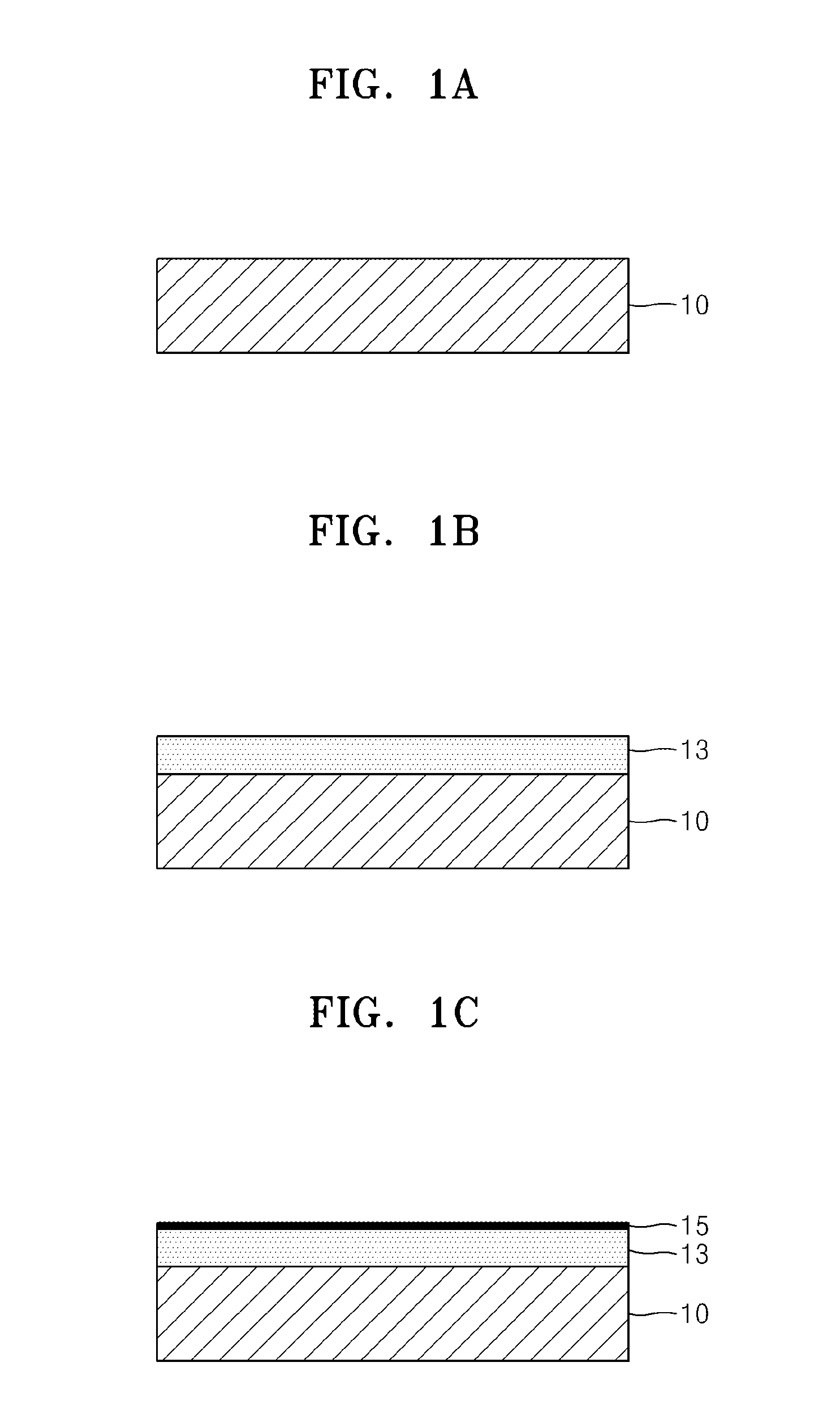
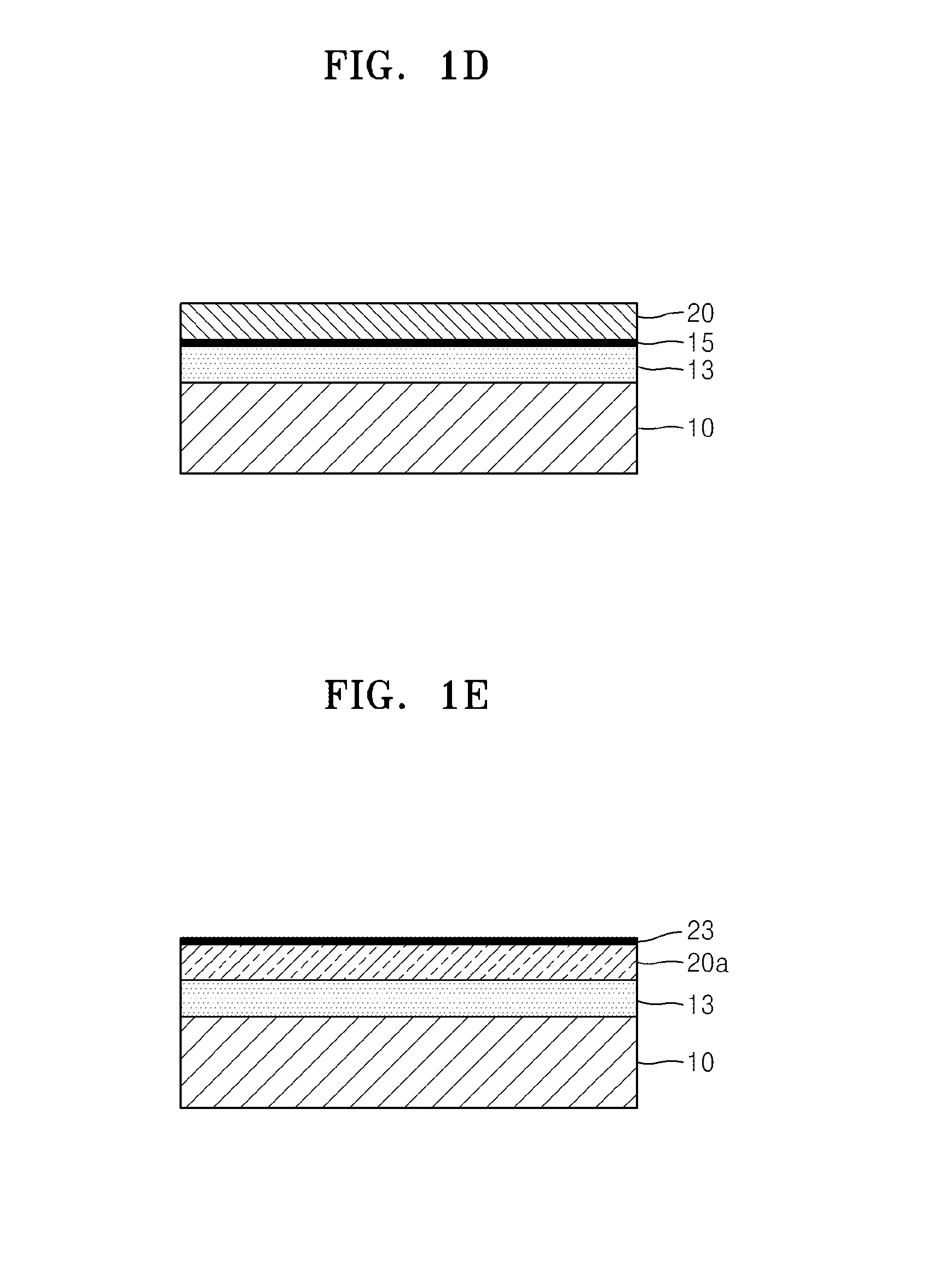
[0025]Reference will now be made in detail to embodiments, examples of which are illustrated in the accompanying drawings, wherein like reference numerals refer to the like elements throughout. In this regard, the present embodiments may have different forms and should not be construed as being limited to the descriptions set forth herein. Accordingly, the embodiments are merely described below, by referring to the figures, to explain aspects of the present description. As used herein, expressions such as “at least one of,” when preceding a list of elements, modify the entire list of elements and do not modify the individual elements of the list.

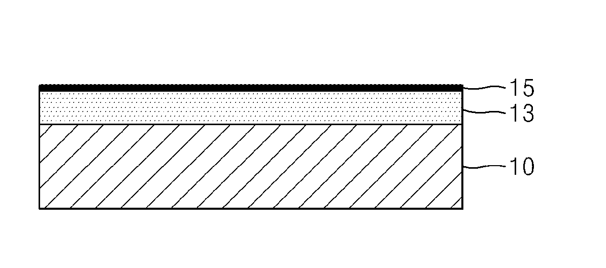
[0026]Hereinafter, semiconductor devices and methods of manufacturing a semiconductor device using a metal oxide according to various example embodiments will be described in detail with reference to the accompanying drawings. The same reference numerals represent the same elements throughout the drawings. In the drawings, the thickness of l...


PUM

PropertyMeasurementUnit
diameteraaaaaaaaaa
semiconductoraaaaaaaaaa
insulatingaaaaaaaaaa

Abstract

A method of manufacturing a semiconductor device using a metal oxide includes forming a metal oxide layer on a substrate, forming an amorphous semiconductor layer on the metal oxide layer, and forming a polycrystalline semiconductor layer by crystallizing the amorphous semiconductor layer using the metal oxide layer.

Description

CROSS-REFERENCE TO RELATED APPLICATIONS[0001]This application claims the benefit of Korean Patent Applications No. 10-2012-0119303, filed on Oct. 25, 2012, and No. 10-2012-0120623, filed on Oct. 29, 2012, in the Korean Intellectual Property Office, the disclosure of each of which is incorporated herein in its entirety by reference.BACKGROUND[0002]1. Field[0003]Some example embodiments relate to semiconductor devices and methods of manufacturing a semiconductor device using a metal oxide.[0004]2. Description of the Related Art[0005]An amorphous silicon layer has higher field effect mobility, can be applied to a high-speed operating circuit, and may be used to fabricate a complementary metal-oxide semiconductor (CMOS) circuit. Thus, the amorphous silicon layer has been widely used to form a semiconductor layer of a semiconductor device, such as a thin film transistor (hereinafter referred to as a ‘TFT’) or a diode.[0006]Polycrystalline silicon may be formed through direct evaporation ...

Claims


Application Information

Patent Timeline
Patent Type & Authority Applications(United States)
IPC IPC(8): H01L21/02H01L29/04
CPCH01L21/02595H01L29/04H01L29/45H01L29/458H01L29/66136H01L29/66757H01L29/66765H01L29/78675H01L29/78678H01L29/78684H01L29/868H01L21/02381H01L21/02422H01L21/02488H01L21/02532H01L21/02672H01L29/045H01L29/16H01L29/161H01L29/78603H01L29/78672
Inventor WENXU, XIANYUYANG, WOO-YOUNGMOON, CHANG-YOULPARK, YONG-YOUNGLEE, JEONG-YUB
Owner SAMSUNG ELECTRONICS CO LTD
Why Eureka
Try Eureka