Method for manufacturing bonded substrate having an insulator layer in part of bonded substrate

a technology of bonded substrate and insulator layer, which is applied in the direction of basic electric elements, electrical apparatus, and semiconductor devices, can solve the problems of deterioration of dram, unsuitable for circuit application of mixed mounting, and high integration, which is the greatest characteristic of dram, so as to reduce the number of fabrication steps and reduce the cost

Active Publication Date: 2014-05-01
SHIN-ETSU HANDOTAI CO LTD
View PDF4 Cites 125 Cited by
  • Summary
  • Abstract
  • Description
  • Claims
  • Application Information

AI Technical Summary

Benefits of technology

[0036]As described above, according to the present invention, the method for manufacturing a bonded substrate having an insulator layer in part of the bonded substrate can be easily provided at a low cost.
[0037]Furthermore, the insulator layer having an optimum thickness can be assuredly formed at an arbitrary position of the substrate to be manufactured in accordance with a shape, a size, properties, and others of a device that is to be formed after manufacture of the substrate.
[0038]Moreover, in case of fabricating a device having a logic circuit, a DRAM, and others mixedly mounted on the same substrate, since a device can be formed at a position of the insulator layer having an optimum film thickness on the substrate, the bonded substrate that enables fabricating the high-performance multi-functionalized device while reducing the number of fabrication steps can be provided.

Problems solved by technology

However, it is considered that mounting both the logic circuit and the DRAM has the following problem.
Therefore, like a cell transistor of a DRAM or a sense amplifier circuit, it is considered that mixed mounting is unsuitable for application to a circuit that has rigorous demands for, e.g., a leak current level or unevenness of a threshold value.
To solve this problem of the floating-body effect, an extraction device region from a body portion and a contact must be provided with respect to an MOSFET pattern and the body potential must be controlled, but there is a problem that a cell area or an area of a sense amplifier unit is thereby greatly increased, and high integration, which is the greatest characteristics of the DRAM, is deteriorated.
However, in regard to any method, there is no detailed description concerning a configuration of the SOI substrate and a configuration of the BOX layer in the SOI region, and a method for more easily manufacturing a partial SOI substrate has been demanded.

Method used


Image

  • Method for manufacturing bonded substrate having an insulator layer in part of bonded substrate
  • Method for manufacturing bonded substrate having an insulator layer in part of bonded substrate
  • Method for manufacturing bonded substrate having an insulator layer in part of bonded substrate

Examples


example 1

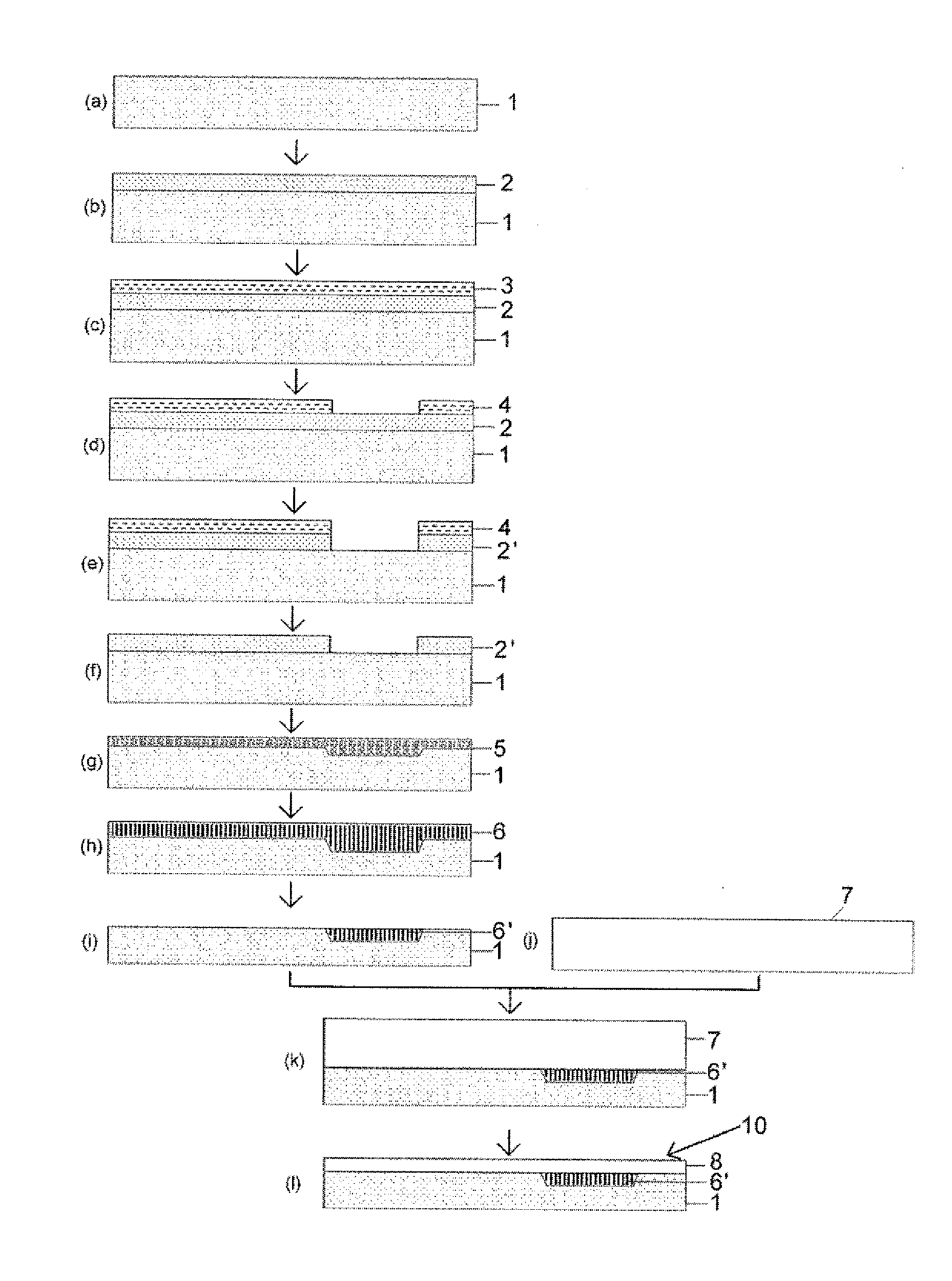
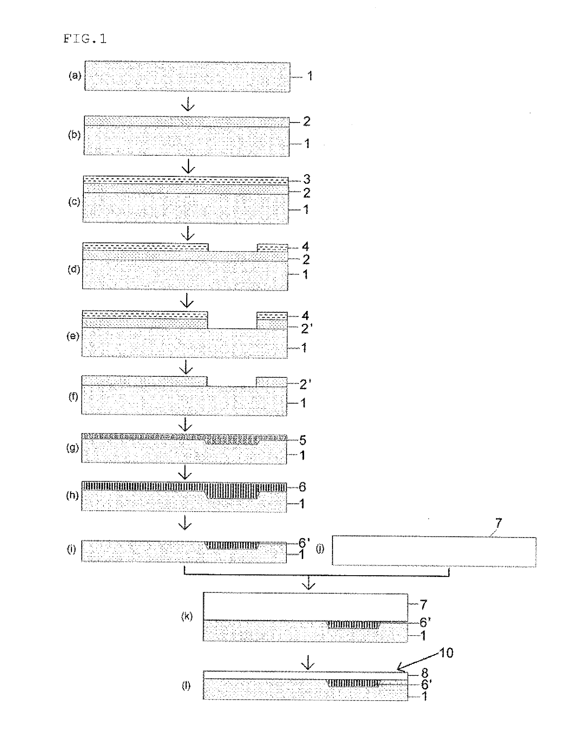
[0075]A boron-doped silicon single crystal substrate having resistivity of 0.05Ω·cm and a diameter of 150 mm was used as a base substrate, a heat treatment was first performed with respect to this substrate at a temperature of 1000° C. in a Pyro atmosphere for 90 minutes, and an oxide film of 200 nm was formed as a protective coat. Then, a resist film was applied to the upper side of the substrate, and a resist mask was formed by photolithography. At this time, as the resist film, a negative resist was selected. An opening portion of a 1 mm square was formed at point where an insulator layer is provided when a bonded substrate is manufactured. In this substrate having the resist mask, the protective coat was etched with a buffered HF solution, the resist mask was removed with use of a mixed liquid of a sulfuric acid and hydrogen peroxide, then RCA cleaning was carried out, and thereby the protective coat was patterned into a shape of the resist mask. This base substrate was subjecte...

example 2

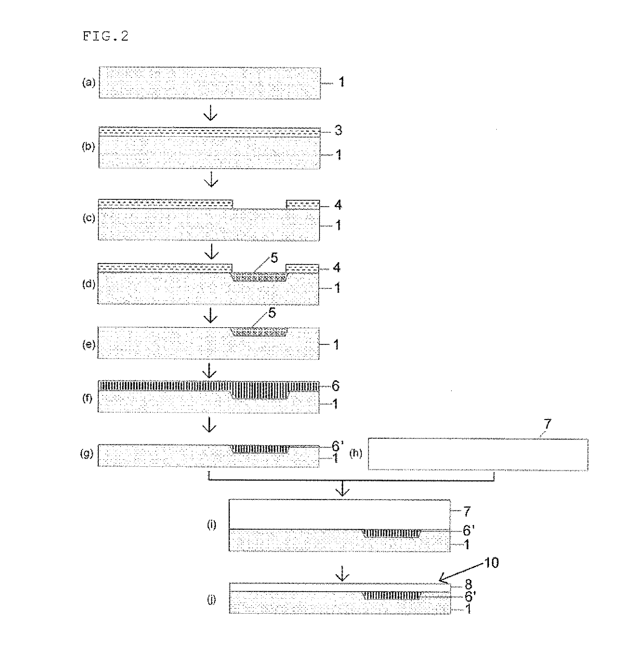
[0077]A boron-doped silicon single crystal substrate having resistivity of 0.05Ω·cm and a diameter of 150 mm was used as a base substrate, a resist film was first applied to the upper side of the substrate, and a resist mask was formed by the photolithography. At this time, as the resist film, a negative resist was selected. An opening portion of a 1 mm square was formed at point where an insulator layer is provided when a bonded substrate is manufactured. This base substrate was subjected to anodic oxidation with HF concentration of 25% and a current application time of 50 seconds, and a porous layer having a thickness of approximately 100 nm and porosity of approximately 40% was formed. A point that was anodically oxidized and a point that was not anodically oxidized were formed on the base substrate since a point where the resist mask is provided is not subjected to the anodic oxidation, and the porous layer was thereby partially formed on a bonding surface of the base substrate....


PUM

PropertyMeasurementUnit
porosityaaaaaaaaaa
thicknessaaaaaaaaaa
porosityaaaaaaaaaa

Abstract

A method for manufacturing a bonded substrate that has an insulator layer in part of the bonded substrate includes: partially forming a porous layer or forming a porous layer whose thickness partially varies on a bonding surface of the base substrate; performing a heat treatment to the base substrate having the porous layer formed thereon to change the porous layer into the insulator layer, and thereby forming the insulator layer whose thickness partially varies on the bonding surface of the base substrate; removing the insulator layer whose thickness varies by an amount corresponding to a thickness of a small-thickness portion by etching; bonding the bonding surface of the base substrate on which an unetched remaining insulator layer is exposed to a bond substrate; and reducing a thickness of the bonded bond substrate and thereby forming a thin film layer.

Description

TECHNICAL FIELD[0001]The present invention relates to a method for manufacturing a bonded substrate having an insulator layer in part of the bonded substrate, which is used for fabrication of a multi-functionalized device such as a device having a logic circuit, a DRAM, and others mixedly mounted thereon.BACKGROUND ART[0002]As a method for improving system performance of LSI, technology for integrating a logic circuit and a DRAM on the same semiconductor chip has been conventionally examined. On the other hand, in a single logic circuit configured mainly based on an MOSFET, to achieve high performance, an SOI-MOSFET using a thin-film SOI substrate in place of a conventional bulk silicon substrate has been examined and already put into production for an intended purpose of some of high-performance logic devices, and its superiority has been proved. In such a situation, taking further improvement of performance into account, development of LSI having a DRAM mixedly mounted on a high-p...

Claims


Application Information

Patent Timeline
Patent Type & Authority Applications(United States)
IPC IPC(8): H01L21/762
CPCH01L21/76251H01L21/76256H01L21/84H01L27/1207
Inventor OHTSUKI, TSUYOSHIQU, WEI FENGTAHARA, FUMIOOOI, YUUKIMITANI, KIYOSHI
Owner SHIN-ETSU HANDOTAI CO LTD
Why Eureka
Try Eureka