

Planar polarization transformer
a transformer and plane polarization technology, applied in the field of plane polarization transformers, can solve the problems of inability to achieve continuous grating lines, inability to achieve transmission te and tm fields being out of phase, and inability to use refractive indexes available in nature at optical frequencies, etc., to achieve the effect of high efficiency, easy manufacturing, and high quality
- Summary
- Abstract
- Description
- Claims
- Application Information
AI Technical Summary
Benefits of technology
Problems solved by technology
Method used
Image

Examples
first embodiment
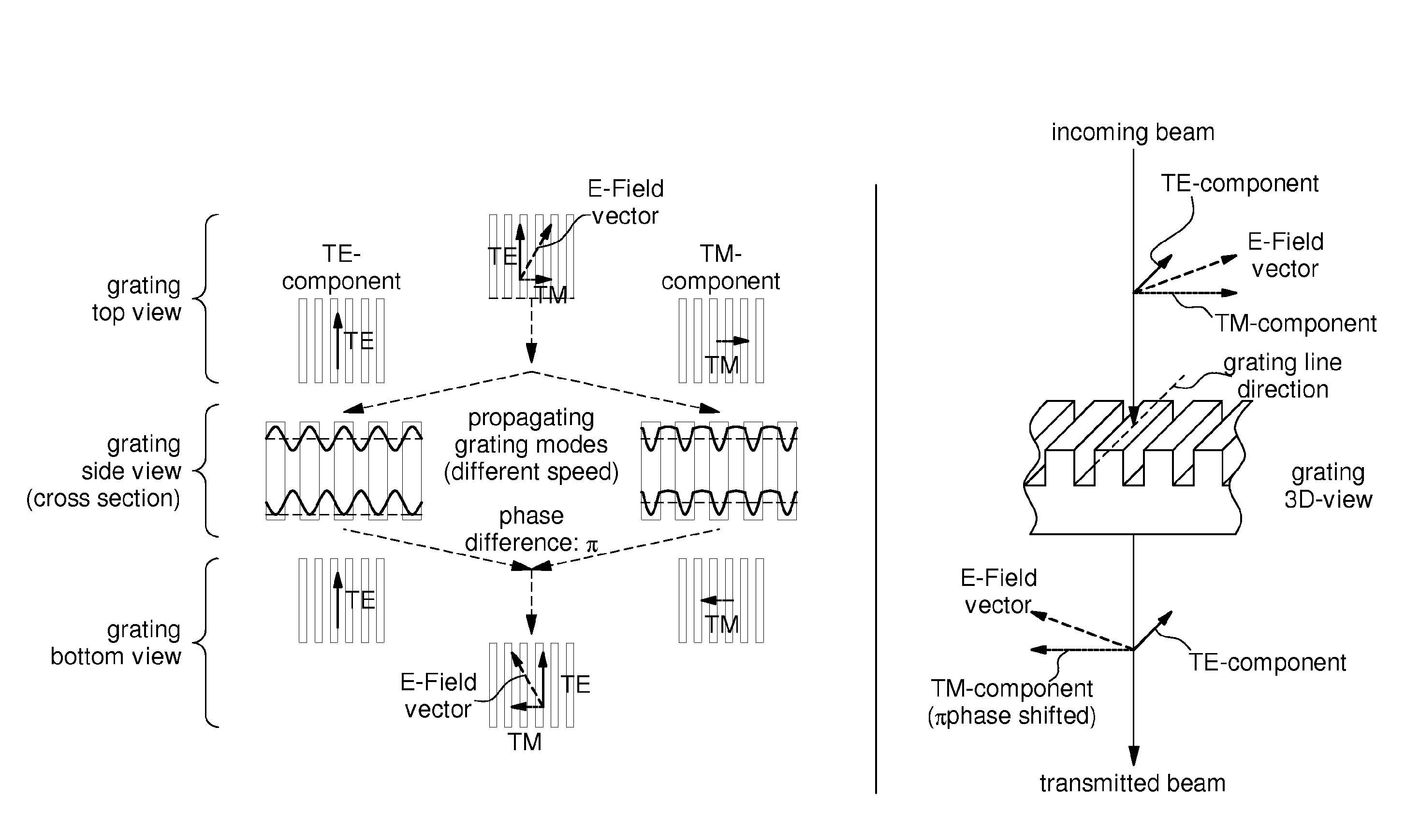
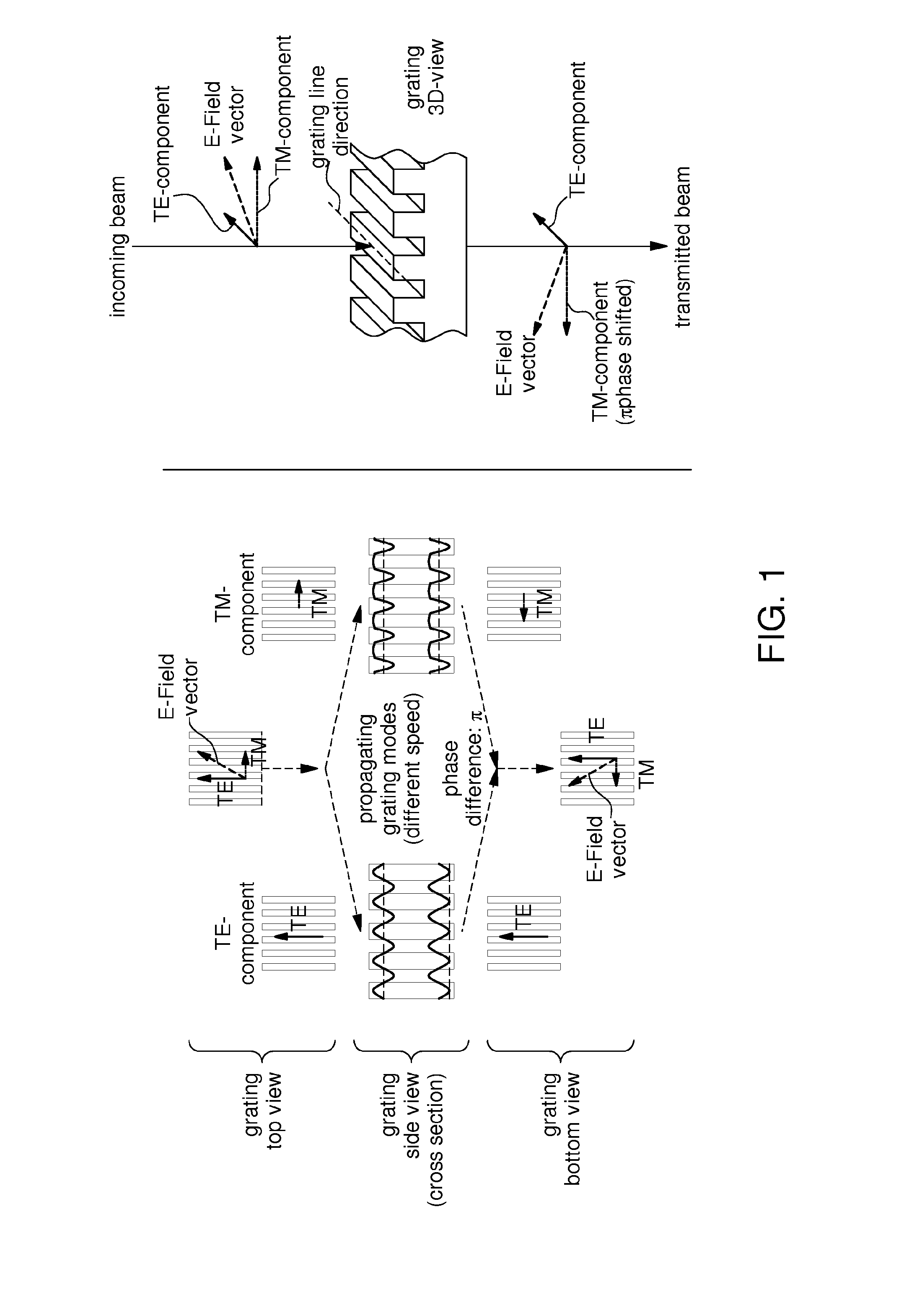
[0048]the invention is partially represented in cross-section in FIG. 5A. The polarization transformer 2 is intended for a light beam or light wave of a given wavelength λ in the optical domain arbitrarily defined as extending from 193 nm up to 20 micrometer vacuum wavelength. This polarization transformer is formed by a planar structure comprising a substrate 4 having refractive index ns and a grating 6 arranged on this substrate. The incidence of the light wave is substantially normal to the planar structure. It can however be off normal (typically up to 5 degrees), as long as no orders higher than the 0th order appear in the substrate. The optical planar grating 6 defines a grating region (also named grating layer or grating medium or grating zone) and is formed by ridges 8 of width Wr and grooves 10 of width Wg forming a corrugation of substantially rectangular profile. This planar grating is located between a cover medium, having a refractive index nc smaller (or lower) than or...
second embodiment
[0049]FIG. 5B shows a polarization transformer 12 according to the invention wherein the transparent substrate is formed by a thick layer 4A of low index material like ThF4 disposed on top of a mechanical substrate (support) of any transparent material, for instance ZnSe, having a larger index ns*(in the case of ZnSe, the index value ns*=2.403 at λ=10.6 μm). The height of the thick layer is chosen so that the optical substrate actually “seen” by the light is essentially ThF4 with ns=1.32. Thus, the low index optical substrate is thick enough to preclude the tunneling of the + / −1st transmitted diffraction orders into the high index support through the low index optically thick substrate layer.
[0050]The evanescent +1st and −1st diffraction orders in the low index optical substrate of index ns have an exponential decay in the direction normal to the plane of the element. The factor in the exponential is −z((λ / Λ)2−ns2)1 / 2)2π / λ where z is the coordinate along the normal with origin at th...
PUM
 Abstract
Description
Claims
Application Information