Semiconductor diode assembly

a technology of semiconductor diodes and diodes, applied in the direction of diodes, semiconductor devices, electrical equipment, etc., can solve the problems of premature damage of heat-damaged tv devices, and achieve the effects of reducing costs, facilitating device packaging, and less complication

Active Publication Date: 2014-06-19
DIODES INC
View PDF2 Cites 5 Cited by
  • Summary
  • Abstract
  • Description
  • Claims
  • Application Information

AI Technical Summary

Benefits of technology

[0009]Other aspects of this invention include introducing dopant into semiconductor material in multiple trenches without covering portions of die with a photo-making material so devices that embody this invention may breakdown symmetrically with respect to the two terminals of the electrical circuit path. One advantage of this is that the devices can be made with less complication and lower cost.
[0010]Another aspect of this invention is that by inserting a masking layer, bi-directional devices with asymmetric breakdown voltages can be realized. And with one further additional masking layer, unidirectional devices, which provide TSV protection in only one direction with respect to the two terminals, can also be realized.
[0011]In summary, the invention enables a person skilled in the art of semiconductor devices to fabricate and use among other implementations, TVS devices that can absorb a larger quantity of energy in the form of a transient voltage surge and recover from it than achievable in the known art because they can achieve junction breakdown voltages closer to the theoretical value and across the entire p-n junction area. Many devices that embody this invention have terminals accessible from their top surface alone and thus facilitate device packaging for low cost and high packing density.

Problems solved by technology

Because junction breakdown under electrical stress induces high current density at the limited area curved portion of the p-n junction, the heat will damage such a TVS device prematurely.

Method used


Image

  • Semiconductor diode assembly
  • Semiconductor diode assembly
  • Semiconductor diode assembly

Examples


example 1

A Symmetrical Bi-Directional Transient Suppressor

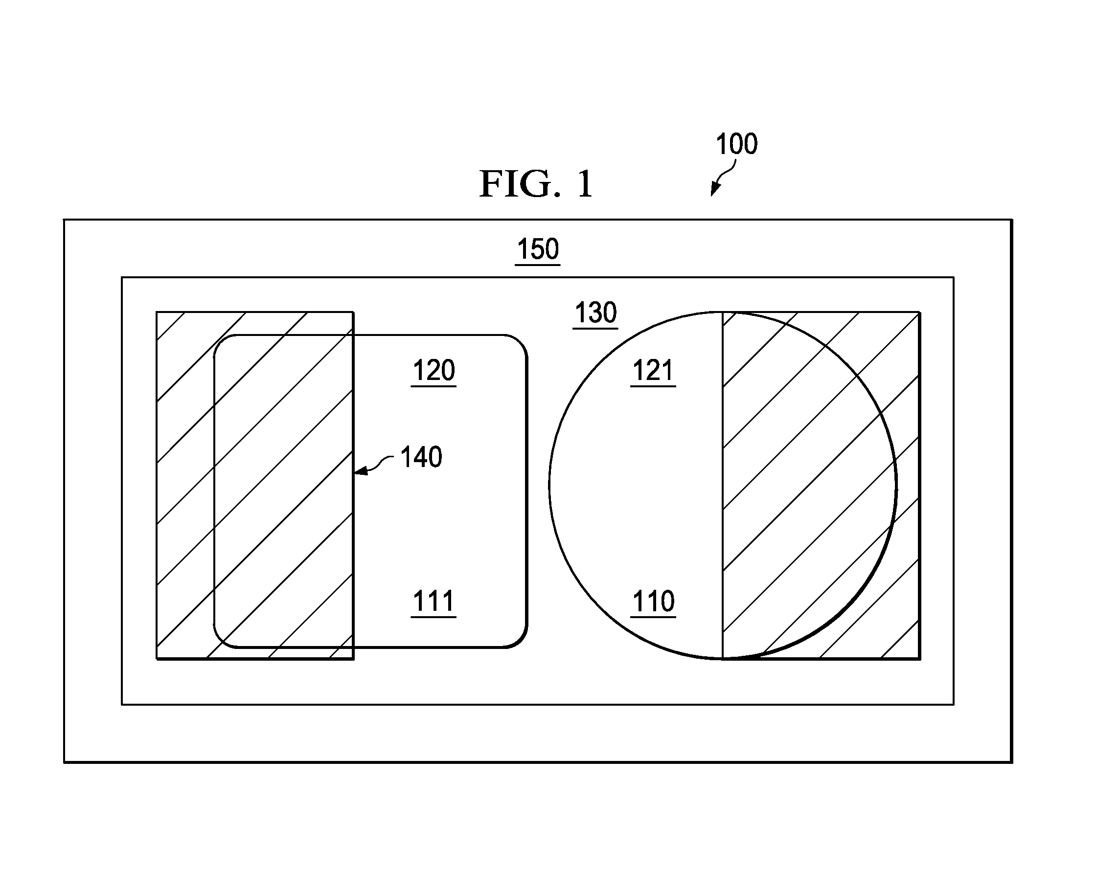
[0019]FIG. 1 depicts the top surface of a partially completed exemplary semiconductor device chip 100 embodying certain aspects of this invention. The chip as depicted has two trenches 110 and 111 located at the middle portion of the chip. Although one circular trench and one square trench are depicted they may be replaced by other shapes such as oval, oblong, polygon and non-geometrical trenches. Each of the trenches 110 and 111 is depicted as fully enclosing a columnar region of the semiconductor material that makes up the device chip 100. In this example, the semiconductor material is silicon but other semiconductor materials such as silicon carbide, gallium nitride, gallium arsenide, etc. are also contemplated.

[0020]The inside diameter of the circular trench of this exemplary device 150 μm, and the trench width is 1.5 μm. Trenches are etched into the silicon chip from its top surface with the chip still a part of a silicon wafer. ...

example 2

An Asymmetrical Bi-Directional Transient Suppressor

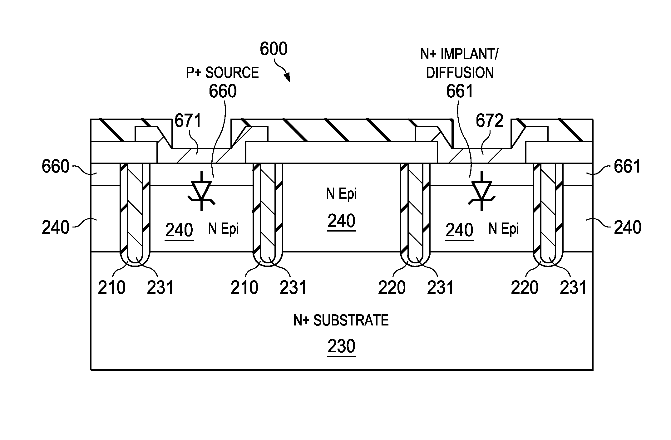
[0034]FIG. 4 depicts another exemplary device 400. The main difference between device 400 and device 300 depicted in FIG. 3 is that the layer 130 in FIG. 3 is absent from the vicinity of the p-n junction diode 401 on the left side of FIG. 4 but is present near the p-n junction on the right side of FIG. 4. This is accomplished with a masking operation that covers the diode area during the ion implant step resulted in the n-layer near the junction diode 411. As a result, the junction breakdown of the diode 411 will be lower by a predictable voltage than that of the diode 401. This device is advantageous in applications where the expected voltage transients are higher with one polarity over the opposite polarity.

example 3

Another Symmetrical Bi-Directional Transient Suppressor

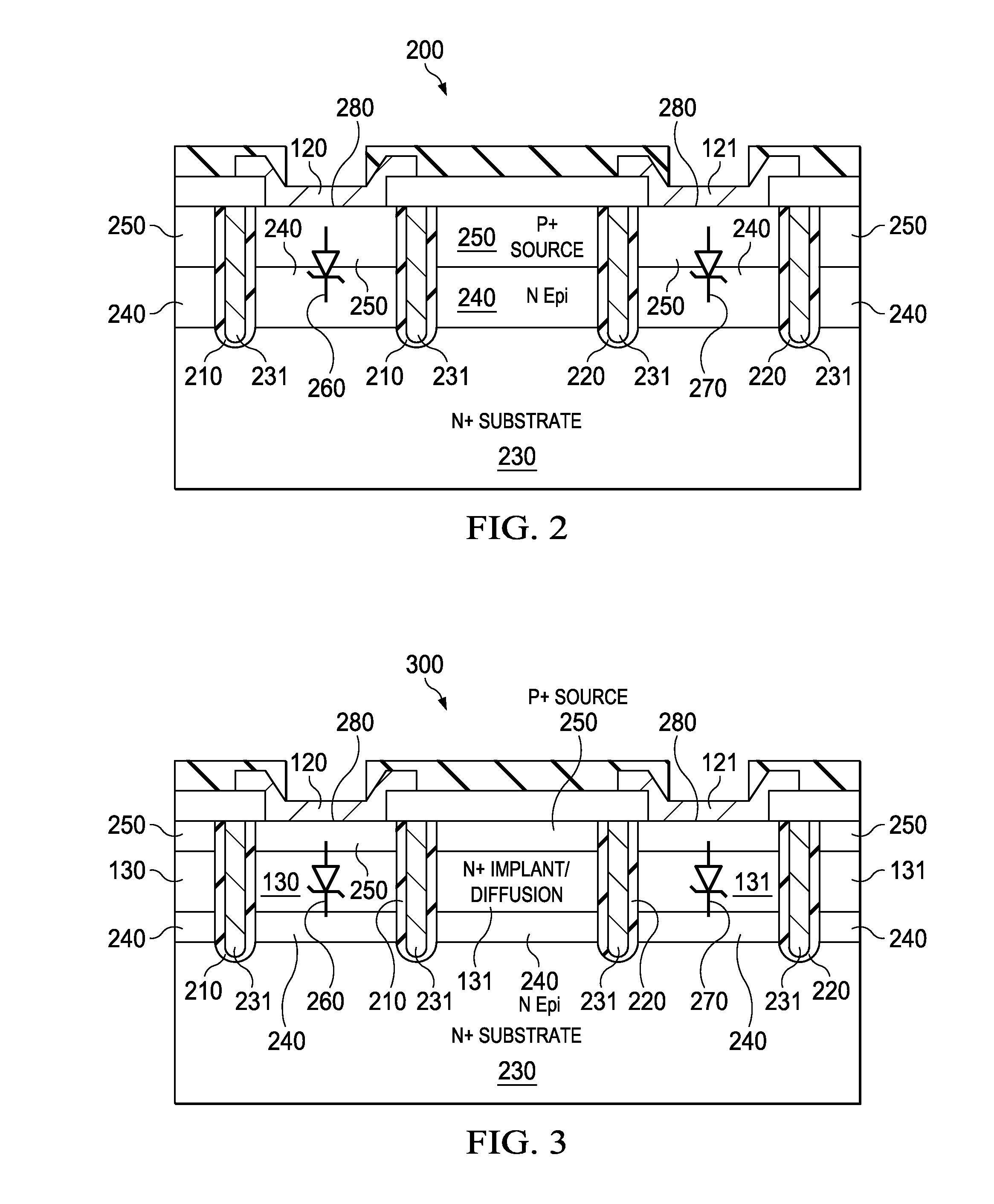
[0035]FIG. 5 depicts yet another exemplary device 500. Device 500 as depicted is a, bi-directional, symmetrical transient suppressor. The main difference between device 500 and device 200 is that in device 500 the substrate 230 and the epitaxial layer 240 are of the opposite doping type while in the device 200, they are of the same polarity.

[0036]As a consequence, the p-n junctions 550 and 551 in device 500 are formed between the substrate and the epitaxial layer. In this exemplary device, as well as in the previous devices, because the diode junctions 500 and 551 are planar, they also are advantageous over non-planar junctions in the known art. Furthermore because the doping concentrations of the substrate and the epitaxial layer can be controlled more tightly than that of the implanted or diffused layer, the control over the junction breakdown voltage may also be tighter.


PUM

PropertyMeasurementUnit
diameteraaaaaaaaaa
angleaaaaaaaaaa
diameteraaaaaaaaaa

Abstract

TSV devices with p-n junctions that are planar have superior performance in breakdown and current handling. Junction diode assembly formed in enclosed trenches occupies less chip area compared with junction-isolation diode assembly in the known art. Diode assembly fabricated with trenches formed after the junction formation reduces fabrication cost and masking steps increase process flexibility and enable asymmetrical TSV and uni-directional TSV functions.

Description

BACKGROUND[0001]Over-voltage transients in the form of electro-static discharge, electromagnetic interference, lighting, or in other harmful forms can strike integrated circuit (IC) packages unexpectedly. Therefore, transient suppressing measures are often necessary to ensure normal functionality over the expected life span of the packaged circuits.[0002]In electronic systems such as cell phones, laptop computers, handheld GPS systems, or digital cameras where space is severely limited, transient voltage suppressor (TVS) devices made of semiconductor are the only viable choice to protect the sensitive IC chips in the systems. To merge the TVS functionality into the chips to be protected is mostly impractical because fabrication processes designed for most integrated circuits do not lend themselves to good TVS performance. For this reason, stand-alone semiconductor TVS devices remain the choice in the industry.[0003]In the TVS devices, p-n junctions and the associated depletion regio...

Claims


Application Information

Patent Timeline
Patent Type & Authority Applications(United States)
IPC IPC(8): H01L29/06H01L21/02
CPCH01L21/02518H01L29/0607H01L29/861H01L27/0255H01L29/36H01L29/66136H01L29/8613
Inventor EARNSHAW, JOHNKEMPER, WOFGANGLIN, YEN-YIBADCOCK, STEVEFRENCH, MARK
Owner DIODES INC
Why Eureka
Try Eureka