

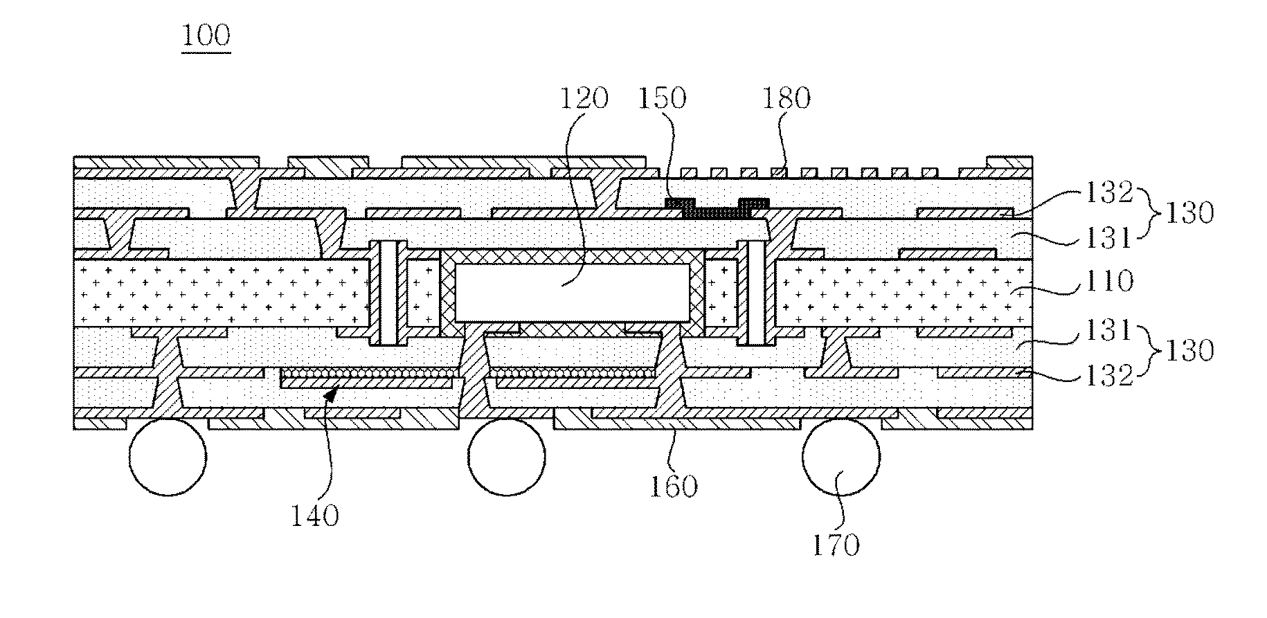
Printed circuit board having copper plated layer with roughness and method of manufacturing the same
a printed circuit board and copper plated technology, which is applied in the direction of insulating substrate metal adhesion improvement, photomechanical equipment, instruments, etc., can solve the problems of uneven adhesive force of insulating pr on copper redistribution layer (rdl), complicated wiring of printed circuit boards, and high density of printed circuit boards. , to achieve the effect of excellent adhesive force and simple and economic method of manufacturing
- Summary
- Abstract
- Description
- Claims
- Application Information
AI Technical Summary
Benefits of technology
Problems solved by technology
Method used
Image

Examples
##ventive example 1
INVENTIVE EXAMPLE 1
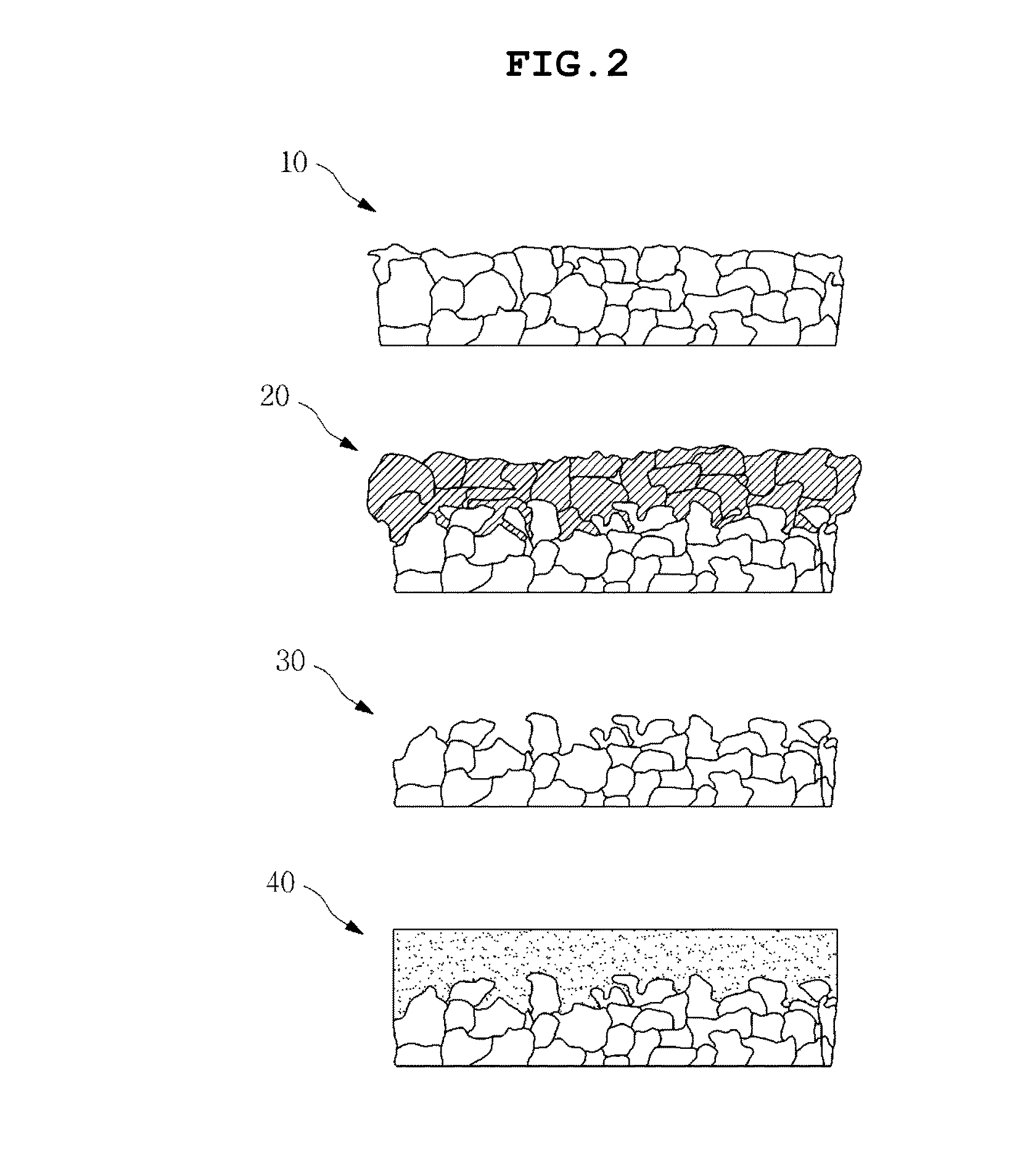
[0068]A board in which a copper film is grown to have a thickness of 8 μm by an electroplating method in an electro plating bath from a copper foil seed layer having an area wider than that of a copper RDL such as copper dummy patterns, ground pattern, and PDN wiring pattern was prepared. Then, a plating photoresist was removed, wet surface cleaning (using acid and water) was performed on the board, and then the board was sufficiently dried at 120° C. for 30 minutes using nitrogen gas or in a vacuum oven. The sufficiently dried board was charged in a vacuum chamber, and basic vacuum was exhausted to 5×10⁻⁷ Torr before working. Next, argon gas is purged, and Cl2 gas and argon or hydrogen gas is supplied into the vacuum chamber to discharge plasma, and then radio frequency (RF) bias is applied to the board. Here, in a system in which gas was configured of Cl2 gas and argon gas, a ratio of argon was adjusted so as not to exceed about 40 vol. %, and in a system in whi...
##ventive example 2
INVENTIVE EXAMPLE 2
[0069]In an electro plating bath, after a plating process of a copper RDL was performed at an average thickness of 8 μm, wet surface cleaning (using acid and water) was performed on the board in a state in which a plating photoresist was not removed, and then the board was sufficiently dried at 120° C. for about 30 minutes using nitrogen gas or in a vacuum oven. The sufficiently dried board was charged in a vacuum chamber, and basic vacuum was exhausted to 5×10⁻⁷ Torr before working. Next, argon is purged, and Cl2 and argon or hydrogen gas is supplied into the vacuum chamber to discharge plasma, and then radio frequency (RF) bias is applied to the board. Here, in a system in which gas was configured of Cl2 gas and argon gas, a ratio of argon was adjusted so as not to exceed about 40 vol. %, and in a system in which the gas was configured of Cl2 gas, hydrogen gas, and argon gas, a ratio of hydrogen was adjusted so as not to exceed about 5 vol. %. The ratio of argon...
PUM
| Property | Measurement | Unit |
|---|---|---|
| arithmetic average roughness | aaaaa | aaaaa |
| roughness Rz | aaaaa | aaaaa |
| vol. % | aaaaa | aaaaa |
Abstract
Description
Claims
Application Information