Strongly correlated nonvolatile memory element

Inactive Publication Date: 2014-07-31
FUJI ELECTRIC CO LTD
View PDF7 Cites 8 Cited by
  • Summary
  • Abstract
  • Description
  • Claims
  • Application Information

AI Technical Summary

Benefits of technology

0025]By means of this mode, first-order transitions between the charge-ordered phase and the orbital-ordered phase of perovskite manganite are possible even i

Problems solved by technology

In recent years there have been concerns that the scaling rule which has been a guiding principle for improvement of semiconductor device performance will finally reach a limit.
On the other hand, there has also been progress made in research on materials having strongly correlated electron systems, to which the band theory which has supported the foundations of semiconductor device design cannot be applied.
Hence the lattice mismatch at the interface between the manganese oxide used in the channel layer and the ferroelectric material which is the gate insulator thereabove becomes too great, and the occurrence of defects in the interface is unavoidable.
If such defects are introduced, leakage currents through

Method used


Image

  • Strongly correlated nonvolatile memory element
  • Strongly correlated nonvolatile memory element
  • Strongly correlated nonvolatile memory element

Examples


Example

First Embodiment

1. Operation Principles

[0051][1-1. Summary Configuration of Memory Element]

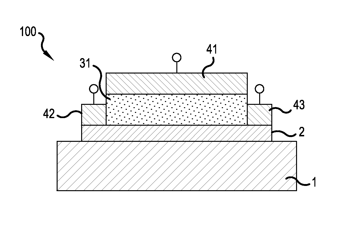
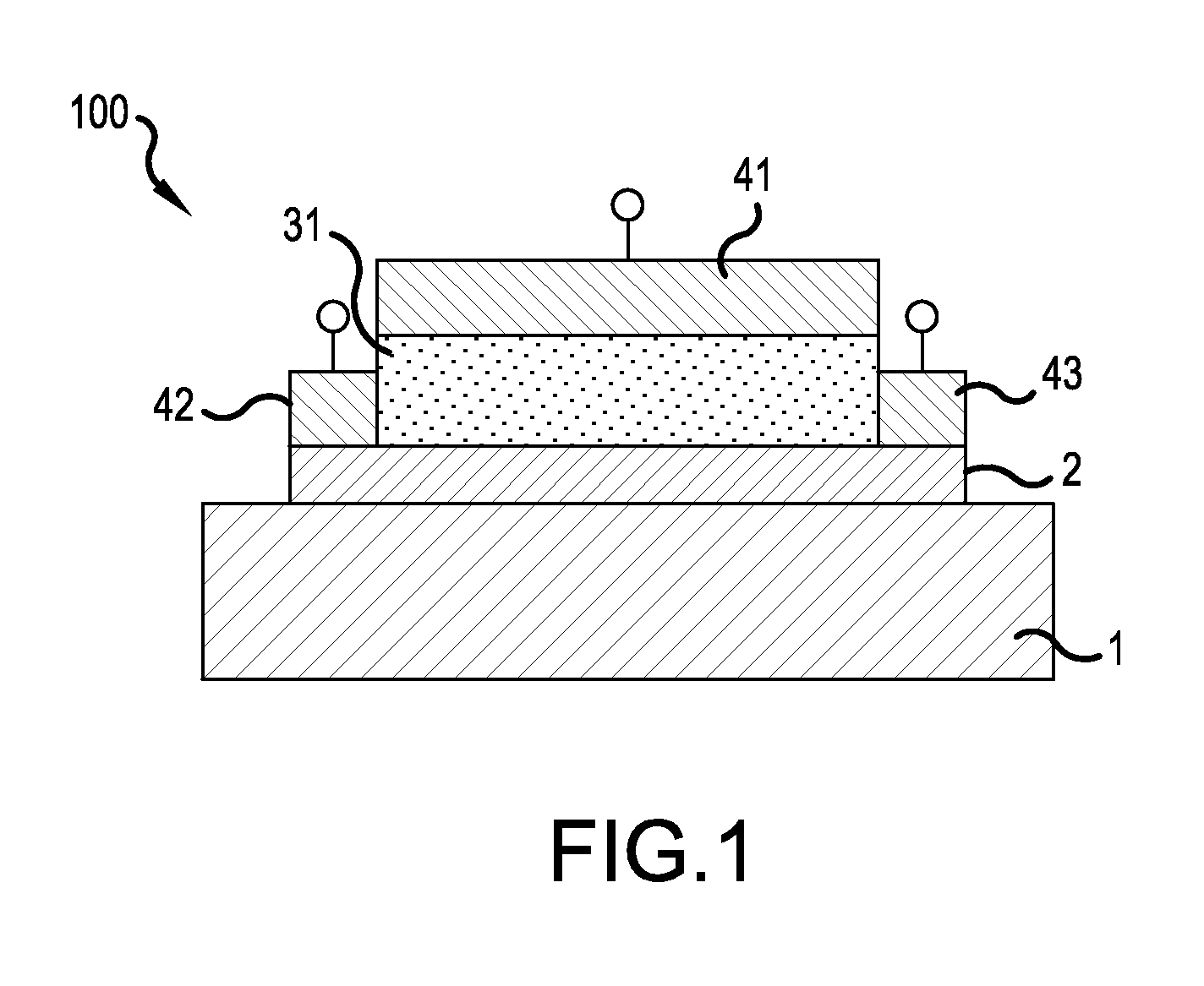
[0052]FIG. 1 is a summary cross-sectional view showing the configuration of a strongly correlated nonvolatile memory element in one example of this embodiment, and shows the structure of a strongly correlated nonvolatile memory element 100 (hereafter called “strongly correlated nonvolatile memory 100”) having a top-gate structure. In FIG. 1, a channel layer 2 including a strongly correlated oxide is formed on the surface of the substrate 1 in the upward direction in the plane of the paper. Throughout this application, other terms including “top-gate structure” and “channel layer” are used to facilitate understanding of the invention of the application by contrast with for example MOSFETs (Metal Oxide Semiconductor Field Effect Transistors) using silicon, which are representative of field-effect elements of the prior art.

[0053][1-2. Switching Mechanism]

[0054]The inventor of this application foc...


PUM


Abstract

In aspects of the invention, a strongly correlated nonvolatile memory element is provided which exhibits phase transitions and nonvolatile switching functions through electrical means. In an aspect of the invention, a strongly correlated nonvolatile memory element is provided including, on a substrate, a channel layer, a gate electrode, a gate insulator, a source electrode, and a drain electrode. The channel layer includes a strongly correlated oxide thin film, and is formed of a perovskite type manganite which exhibits a charge-ordered phase or an orbital-ordered phase; the gate insulator is formed in contact with at least a portion of a surface or interface of the channel layer and is sandwiched between the channel layer and the gate electrode, and the source electrode and drain electrode are formed in contact with at least a portion of the channel layer.

Description

CROSS-REFERENCE TO RELATED CASES[0001]This application is a continuation of International Application No. PCT / JP 2012 / 073640, filed on Sep. 14, 2012, which is based on and claims priority to Japanese Patent Application No. JP 2011-230068, filed on Oct. 19, 2011. The disclosure of the Japanese priority application and the PCT application in their entirety, including the drawings, claims, and the specification thereof, are incorporated herein by reference.BACKGROUND[0002]1. Field of the Invention[0003]This invention relates to a strongly correlated nonvolatile memory element. More specifically, this invention relates to a strongly correlated nonvolatile memory element which exhibits nonvolatile memory functions by electrical means.[0004]2. Related Art[0005]In recent years there have been concerns that the scaling rule which has been a guiding principle for improvement of semiconductor device performance will finally reach a limit. These concerns have been accompanied by work to develo...

Claims


Application Information

Patent Timeline
IPC IPC(8): H01L45/00
CPCH01L45/1206H01L45/147G11C11/5685G11C13/0002G11C13/0007G11C2213/53H01L27/101H01L29/7869H01L29/78696H10N70/253H10N70/20H10N70/8836H10N50/10H10N70/235
Inventor OGIMOTO, YASUSHI
Owner FUJI ELECTRIC CO LTD
Why Eureka
Try Eureka