Silicon dioxide-polysilicon multi-layered stack etching with plasma etch chamber employing non-corrosive etchants

a technology of polysilicon dioxide and etching chamber, which is applied in the manufacture of microstructured devices, electrical equipment, electrical discharge tubes, etc., can solve the problems of inherently difficult to etch both films with a single plasma etching system, particularly in the manufacture of such devices, and the difficulty of etching a 3d nand bi-layer stack

Active Publication Date: 2014-07-31
APPLIED MATERIALS INC
View PDF3 Cites 15 Cited by
  • Summary
  • Abstract
  • Description
  • Claims
  • Application Information

AI Technical Summary

Problems solved by technology

While the 3D NAND holds much promise for further scalability (e.g. potentially enabling terabit cell arrays), even in lieu of further lithographic advancement, manufacture of such a device is challenging particularly with respect to forming the vertical features (e.g., plugs) extending through the many gate electrode layers.
Compositional differences of the materials in the bi-layers, make etching a 3D NAND bi-layer stack even more challenging.
However, most plasma etch systems are designed to etch either one, but not both of these materials.
Indeed, systems which etch silicon dioxide well typically do so with very high selectivity to polysilicon while the converse is true for conductor etch systems, making it inherently difficult to etch both films with a single plasma etch system.

Method used


Image

  • Silicon dioxide-polysilicon multi-layered stack etching with plasma etch chamber employing non-corrosive etchants
  • Silicon dioxide-polysilicon multi-layered stack etching with plasma etch chamber employing non-corrosive etchants
  • Silicon dioxide-polysilicon multi-layered stack etching with plasma etch chamber employing non-corrosive etchants

Examples


Embodiment Construction

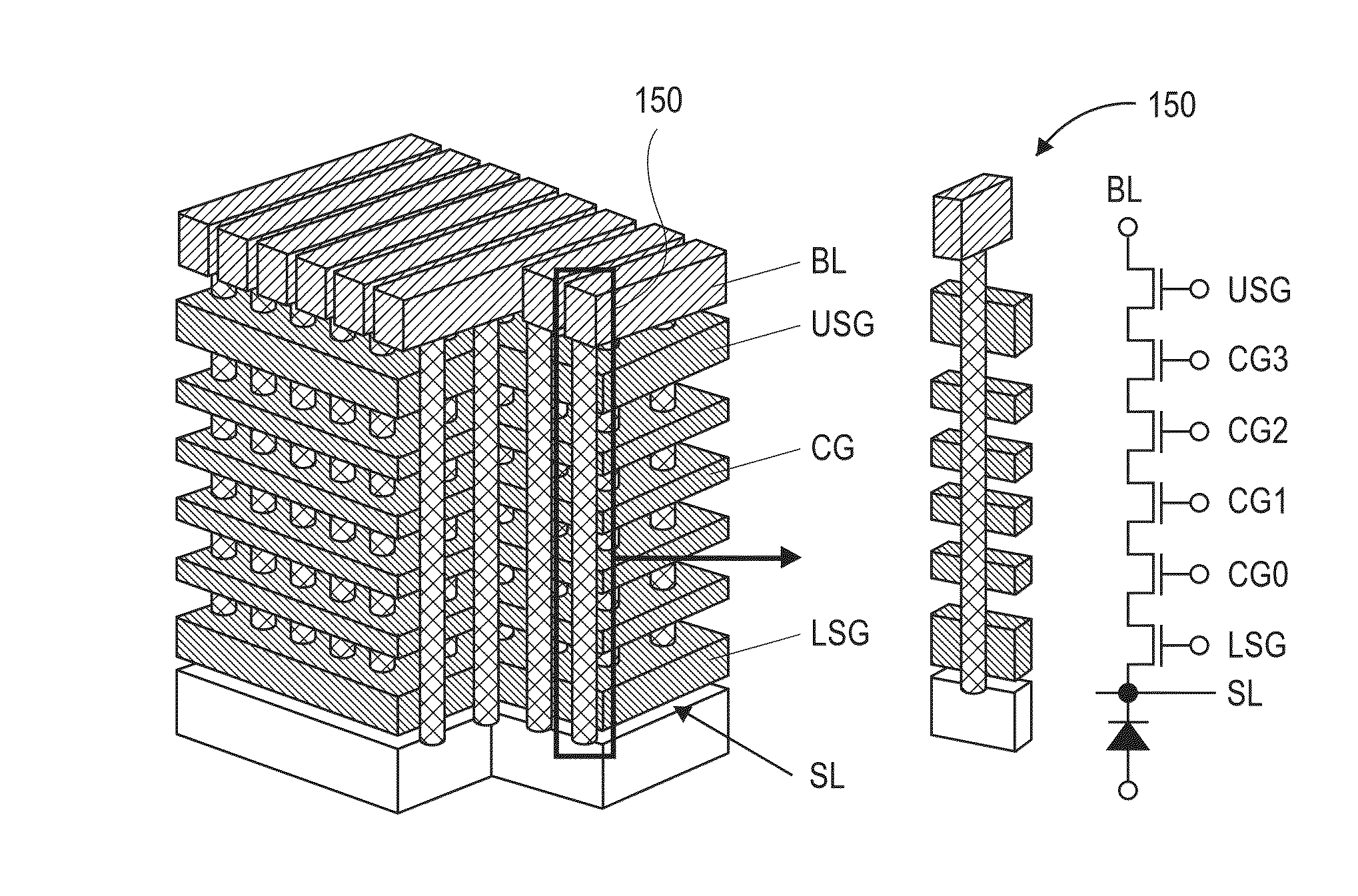
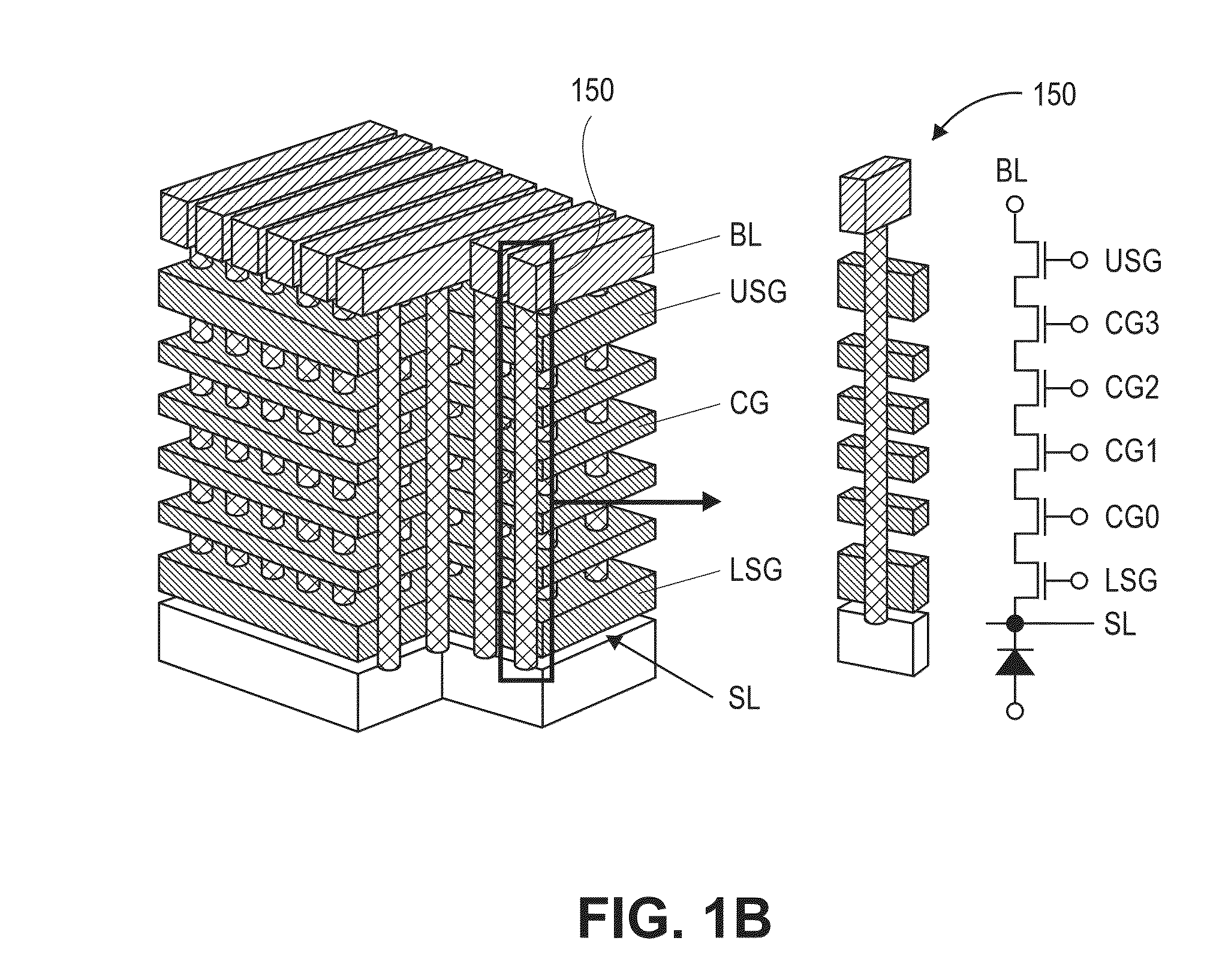
[0022]Multilayered stacks having layers of silicon interleaved with layers of a dielectric, such as silicon dioxide, are plasma etched with non-corrosive process gas chemistries. In the following description, numerous specific details are set forth, such as plasma chamber hardware, gas chemistries, and process sequences, in order to provide a thorough understanding of embodiments of the present invention. It will be apparent to one skilled in the art that embodiments of the present invention may be practiced without these specific details. In other instances, well-known aspects, such as integrated circuit fabrication, are not described in detail in order to not unnecessarily obscure embodiments of the present invention. Furthermore, it is to be understood that the various embodiments shown in the Figures are illustrative representations and are not necessarily drawn to scale.

[0023]In embodiments, non-corrosive gases are employed to etch both silicon and dielectric layers of a stack ...


PUM


Abstract

Multilayered stacks having layers of silicon interleaved with layers of a dielectric, such as silicon dioxide, are plasma etched with non-corrosive process gas chemistries. Etching plasmas of fluorine source gases, such as SF6 and / or NF3 typically only suitable for dielectric layers, are energized by pulsed RF to achieve high aspect ratio etching of silicon / silicon dioxide bi-layers stacks without the addition of corrosive gases, such as HBr or Cl2. In embodiments, a mask open etch and the multi-layered stack etch are performed in a same plasma processing chamber enabling a single chamber, single recipe solution for patterning such multi-layered stacks. In embodiments, 3D NAND memory cells are fabricated with memory plug and / or word line separation etches employing a fluorine-based, pulsed-RF plasma etch.

Description

PRIORITY[0001]This application is a Non-Provisional of, claims priority to, and incorporates by reference in its entirety for all purposes, the U.S. Provisional Patent Application No. 61 / 757,027 filed Jan. 25, 2013.TECHNICAL FIELD[0002]Embodiments of the present invention pertain to the field of semiconductor processing and, in particular, to methods of plasma etching multi-layered films comprising both silicon and dielectric layers.DESCRIPTION OF RELATED ART[0003]Memory chips comprise a large fraction of the semiconductor devices manufactured. One popular semiconductor memory technology is NAND EEPROM (flash), a schematic of which is illustrated in FIG. 1A. Generally, a 16-bit unit of NAND includes a string of 18 transistors. With limitations in lithography becoming more problematic with each dimensional shrink, current trends in semiconductor device scaling include three dimensional (3D) device design. FIG. 1B illustrates one exemplary 3D NAND architecture whereby the transistor s...

Claims


Application Information

Patent Timeline
Patent Type & Authority Applications(United States)
IPC IPC(8): H01L21/3065
CPCH01L21/3065H01L21/31116H01L21/31122H01L21/32137H01J37/32146H01J37/32165H10B41/27H10B43/27B81C1/00531H01L21/67069H01L21/0332H01L21/3081H01L21/31138H01L21/32139H01J37/32082H01J37/3244
Inventor SHIMIZU, DAISUKEKIM, JONG MUN
Owner APPLIED MATERIALS INC
Why Eureka
Try Eureka