

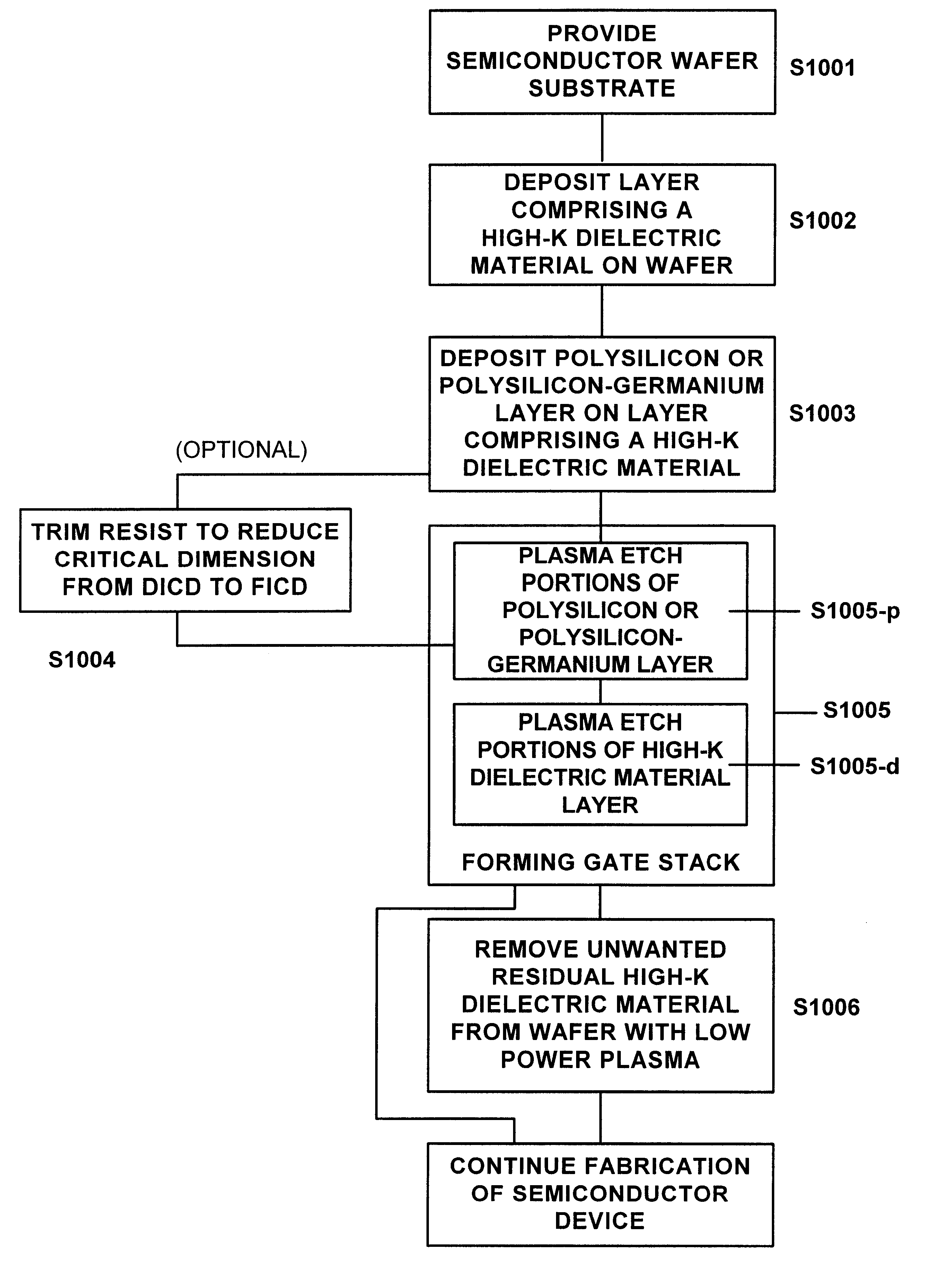
Integrated plasma etch of gate and gate dielectric and low power plasma post gate etch removal of high-K residual
a technology of integrated plasma etching and gate dielectric, which is applied in the direction of semiconductor devices, electrical equipment, transistors, etc., can solve the problems of new methods of fabrication or new arrangements, charge carriers that tunnel across the gate oxide layer, and "leaky transistors" to achieve the effect of reducing the number of steps in the fabrication process, reducing the number of steps, and improving performan
- Summary
- Abstract
- Description
- Claims
- Application Information
AI Technical Summary
Benefits of technology
Problems solved by technology
Method used
Image

Examples
Embodiment Construction
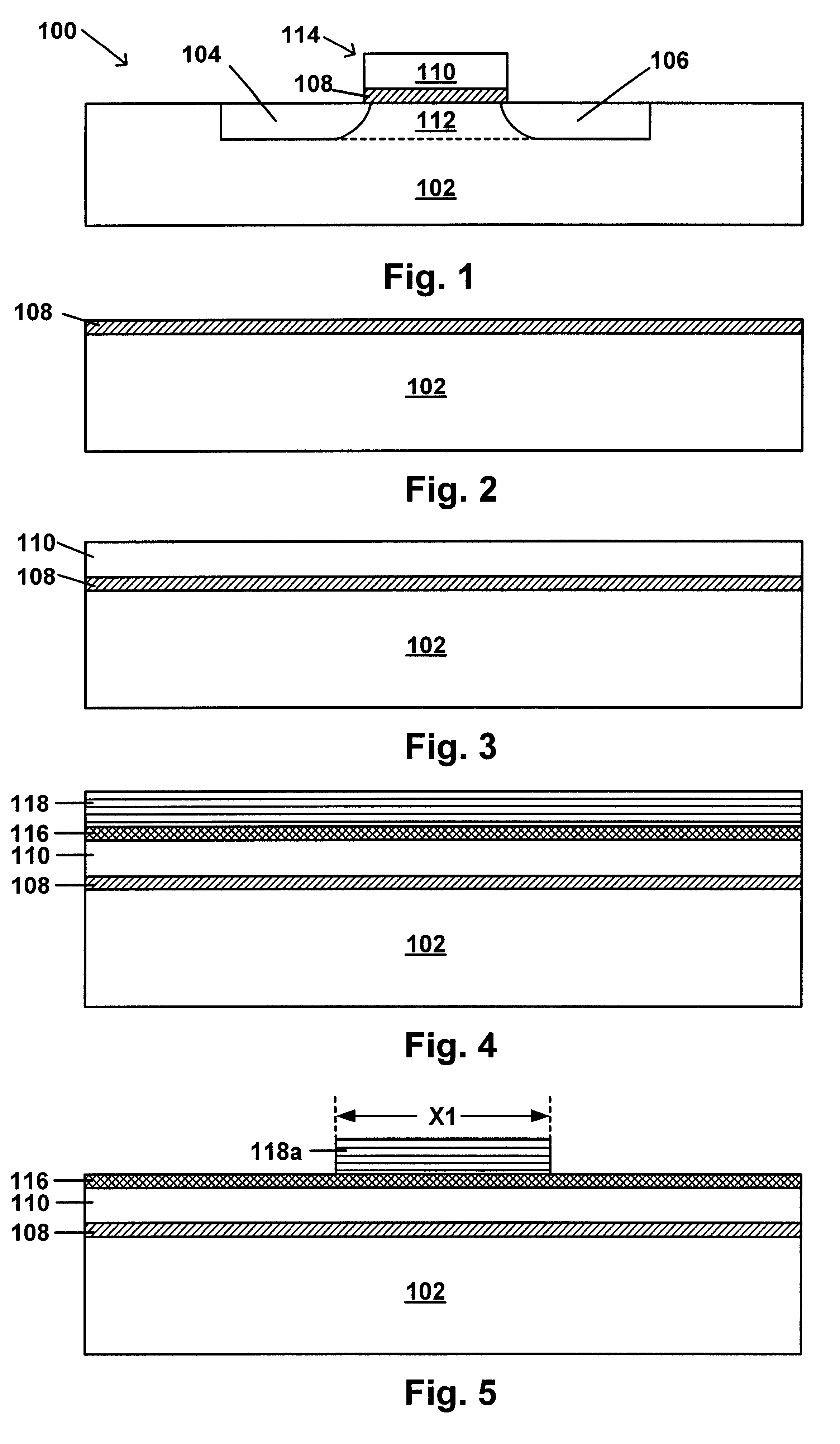
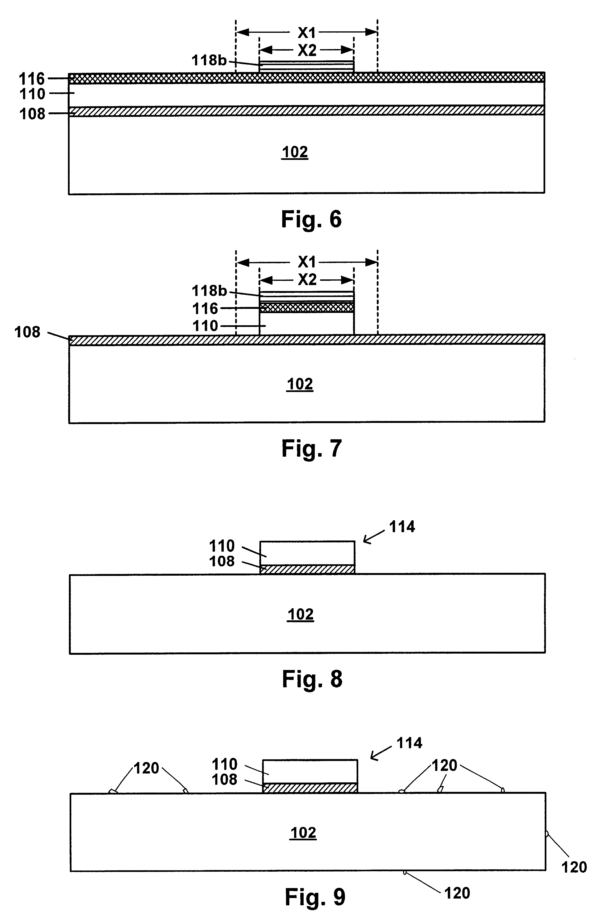
As used herein, the term "standard-K dielectric material" refers to a dielectric material having a dielectric constant, K, up to about 10. Such standard-K dielectric materials include, for example, silicon dioxide, having a K of about 4, silicon oxynitride, having a K of about 4-8 depending on the relative content of oxygen and nitrogen, and silicon nitride, having a K of about 6-9, and aluminum oxide, having a K of about 10.
As used herein, the term "high-K dielectric material" refers to a dielectric material having a dielectric constant, K, greater than about 10. Such high-K dielectric materials include, for example, HfO.sub.2, ZrO.sub.2 and others known in the art, some of which are specifically identified more fully below. In general, the term "high-K dielectric material" encompasses binary, ternary and higher oxides and any ferroelectric material having a K of about 10 or more. High-K dielectric materials may also include, for example, composite materials such as hafnium silicat...
PUM
 Abstract
Description
Claims
Application Information