Unlock instant, AI-driven research and patent intelligence for your innovation.

Radiation detector

Inactive Publication Date: 2014-09-04
INT CRYSTAL LAB
View PDF11 Cites 0 Cited by
  • Summary
  • Abstract
  • Description
  • Claims
  • Application Information

AI Technical Summary

Benefits of technology

The present invention is a device or system that detects radiation using a special crystal called Cd1-xMgxTe. This crystal can be combined with electrodes and other components to create a functional device that works at room temperature. The use of the Cd1-xMgxTe crystal helps to increase the yield of the device and increase the lifespan of the electron and hole components. Additionally, the device can also be designed to amplify, measure, identify, or image the radiation it detects.

Problems solved by technology

The promise of semiconductor based radiation detectors has not been fully met despite high demand for such detectors in many areas, including homeland security, medical imaging, spectroscopy and astrophysics, because the most promising semiconductor materials for this application do not produce high crystal growth yields while those materials that produce high yields do not possess ideal material properties.
Stress creates defects on the polished surface of crystals which may be the source of recombination of electrons and holes, trapping centers and also a source of reduced resistivity at the perimeter which could create current noise.
However, a germanium detector has a small energy bandgap (0.67 eV), and this disadvantage requires that the detector be continuously cooled, making it useless at room temperature and limiting its applicability to portable detector devices.
HgI2 has an energy bandgap 2.13 eV and therefore can operate at room temperature, but it suffers from several shortcomings including a surface that becomes degraded after use for a short time making it impractical to employ as a commercial detector.
484-486) Recently developed CdMnTe has a bandgap of 1.57 eV and has promise for detector applications but it still suffers from very poor crystalline perfection.
However, the widespread deployment of CZT detectors is impeded by high-cost yields due to limited high-quality and large-volume single crystals.
(Balboa, O. S., Surface and Bulk Defects in Cadmium Zinc Telluride and Cadmium Manganese Telluride Crystals, Doctoral Dissertation, Vanderbilt University (2009)) These disadvantages are pre-determined by the mismatch of the lattice constant of CdTe and ZnTe (0.648 nm and 0.610 nm) and the high segregation coefficient of Zn in CdTe (1.35), both of which tend to create crystal defects such as twins and in-homogeneities.
Although a higher concentration of Zn would produce a bigger bandgap closer to the 1.7 eV ideal, crystal growth technical problems have made higher Zn concentration unachievable.

Method used


Image

  • Radiation detector
  • Radiation detector
  • Radiation detector

Examples


example 1

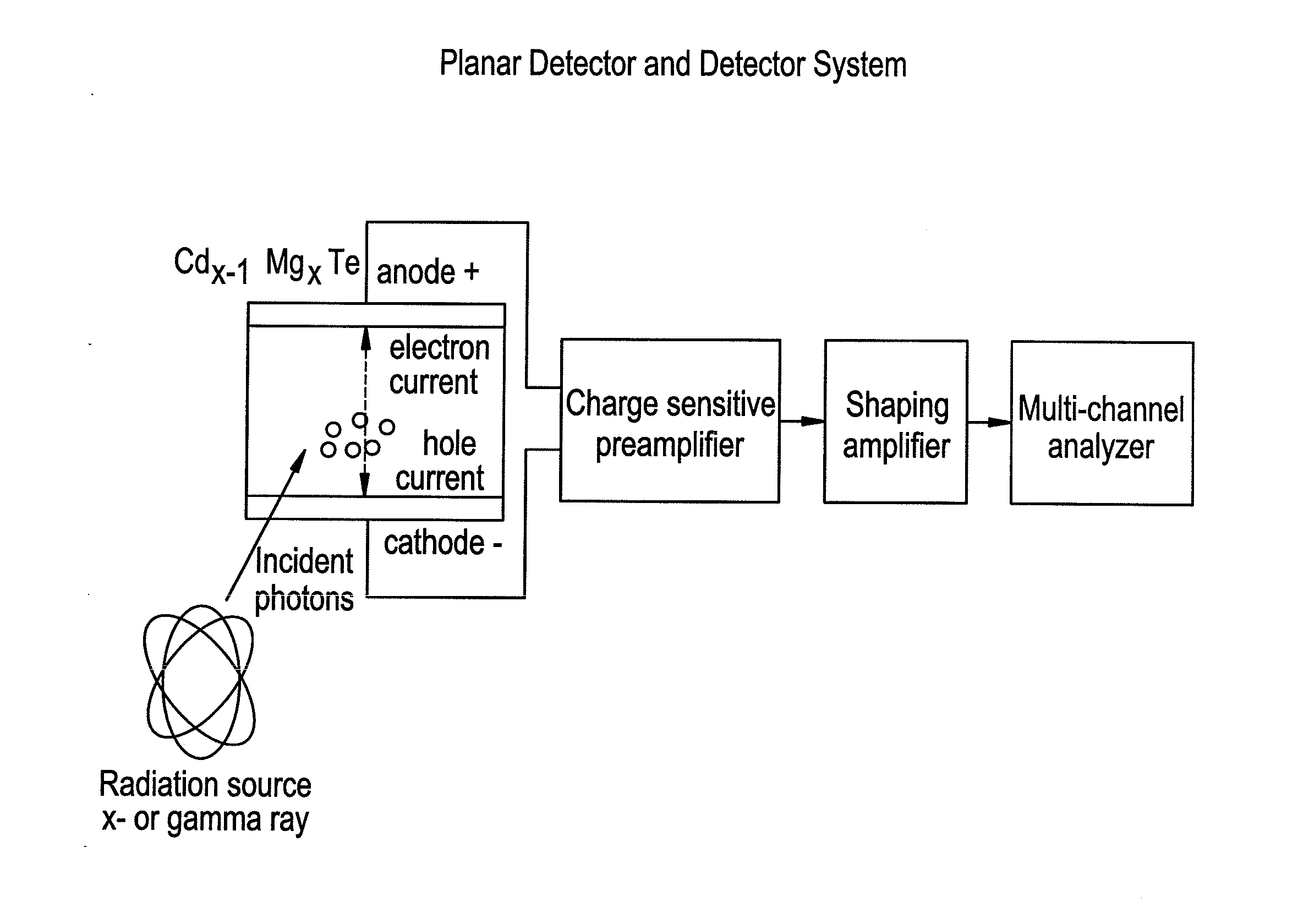
[0055]Crystals were grown by the zone melting with solvent method. An In-doped ingot Cd0.92Mg0.08Te 18 mm diameter 34 mm length was grown with excess Te. The growth was carried out as described above. The ingot was mostly single crystal with very good crystalline perfection. From the single crystal thus grown samples were manufactured which had high resistivity 2×10¹⁰ ohm·cm (FIG. 8). Samples were fabricated into 8×7×3 mm planar detector configured and as shown in FIG. 7 a good spectral response was achieved at 3 voltages (200 v, 250 v, and 300 v) from 241 Am, a commonly used gamma ray source for energy calibration (Glemen F. Knoll, Radiation Detection and Measurement, John Wiley &Sons 2000, p. 486 488) and the electron mobility-lifetime value was determined to be 7×10⁻⁴V / cm2 (FIG. 9).

example 2

[0056]Crystals were grown by the zone melting with solvent method. An In-doped ingot Cd0.95Mg0.05Te 20 mm diameter 42 mm length was grown with excess Te. The growth was carried out as described above. The ingot was mostly single crystal with very good crystalline perfection. From the single crystal thus grown samples were manufactured which had high resistivity 3×10¹⁰ ohm·cm. Samples were fabricated in 8×7×3 mm planar configured in the same manner as Example 1 above. It was confirmed that the detector had a good spectral response from a 241 Am source, and the electron mobility-lifetime value was determined to be 8×10⁻⁴ V / cm2.

example 3

[0057]Crystals were grown by the zone melting with solvent method. An In-doped ingot Cd0.71Mg0.29Te 18 mm diameter 34 mm length was grown with excess Te. The growth was carried out as described above. The ingot was mostly single crystal with very good crystalline perfection. The calculated band gap at this composition is 2.0 eV.

[0058]Crystals were grown by the zone melting with solvent method. An In-doped ingot Cd0.70Mg0.30Te 18 mm diameter 34 mm length was grown with excess Te. The growth was carried out as described above. The ingot had a poor crystalline perfection. Similarly bad crystalline perfection was demonstrated with the composition Cd0.69Mg0.31Te. Cd1-xMgxTe solid solutions in with concentrations of Mg in excess of Cd0.70Mg0.30Te exhibit some evidence of wurtzite structure coexisting with zinc blend. This structure creates flaws which our as grown examples demonstrate preclude single crystal growth of a perfect zinc blend structure at concentration 30 at. % and higher.

[00...


PUM


Abstract

The present invention provides a radiation detection system for detecting X-ray and gamma rays featuring Cd1-xMgx Te in solid solution as a crystal semiconductor and electrical connection means. The crystal has a composition in the range of Cd0.99Mg0.01Te to Cd0.71Mg0.29Te and may be doped with indium or another Group III element, which may be suitable for use at room temperature as well as controlled temperatures. The present invention further provides a method for detecting X- or gamma ray radiation by (a) providing a solid solution Cd1-xMgxTe crystal in the composition range of Cd0.99Mg0.01Te to Cd0.71Mg0.29Te; (b) providing an electrical contact means for connecting the Cd1-xMgxTe crystal to an amplification, measurement, identification or imaging means; and (c) detecting the presence of the X- or gamma ray radiation.

Description

FIELD OF THE INVENTION[0001]The present invention is in the field of semiconductor detectors, especially semiconductor detectors suitable for detecting X-ray and gamma ray radiation at room temperature.BACKGROUND OF THE INVENTION[0002]The promise of semiconductor based radiation detectors has not been fully met despite high demand for such detectors in many areas, including homeland security, medical imaging, spectroscopy and astrophysics, because the most promising semiconductor materials for this application do not produce high crystal growth yields while those materials that produce high yields do not possess ideal material properties. (Balboa, O. S., Surface and Bulk Defects in Cadmium Zinc Telluride and Cadmium Manganese Telluride Crystals, Doctoral Disertation, Vanderbilt University (2009))[0003]Semiconductor radiation detectors are the most recent type of detectors developed, and they are very useful because they convert X-ray and gamma quantum (photons) directly into electri...

Claims


Application Information

Patent Timeline
IPC IPC(8): G01T1/24H01L31/08H01L31/0296
CPCG01T1/24H01L31/085H01L31/02966H01L31/02963H01L31/1832H01L31/1864
Inventor HERPST, ROBERT D.YAKIMOVICH, VLADIMIR
Owner INT CRYSTAL LAB
Features
  • R&D
  • Intellectual Property
  • Life Sciences
  • Materials
  • Tech Scout
  • Unparalleled Data Quality
  • Higher Quality Content
  • 60% Fewer Hallucinations
Learn More