Photoconductive antennas, method for producing photoconductive antennas, and terahertz time domain spectroscopy system

Inactive Publication Date: 2014-09-11
CANON KK
View PDF4 Cites 16 Cited by
  • Summary
  • Abstract
  • Description
  • Claims
  • Application Information

AI Technical Summary

Benefits of technology

[0014]A photoconductive antenna according to an aspect of the invention is a photoconductive antenna that generates and detects a terahertz wave. The photoconductive antenna has a substrate, a buffer layer, a first semiconductor layer, a second semiconductor layer, and an electr

Problems solved by technology

This causes various problems while THz waves pass through the SI—GaAs substrate, such as reduced efficiency of use of the power of the THz waves and spectral narrowing, because of the absorption of near-8-THz waves by TO phonons.
The preceding studies, however, focused on reducing the dislocation density and increasing the area of the growth substrate and were not necessarily to find out a crystal growth technique that could be applied to photoconductive antennas suitable for the generation and detection of THz waves.
The above review article describes a technology that uses Ge as a buffer while growing GaAs, and this approach is known to be disadvantageous because

Method used


Image

  • Photoconductive antennas, method for producing photoconductive antennas, and terahertz time domain spectroscopy system
  • Photoconductive antennas, method for producing photoconductive antennas, and terahertz time domain spectroscopy system
  • Photoconductive antennas, method for producing photoconductive antennas, and terahertz time domain spectroscopy system

Examples


embodiment 1

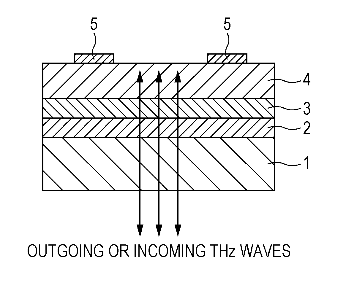
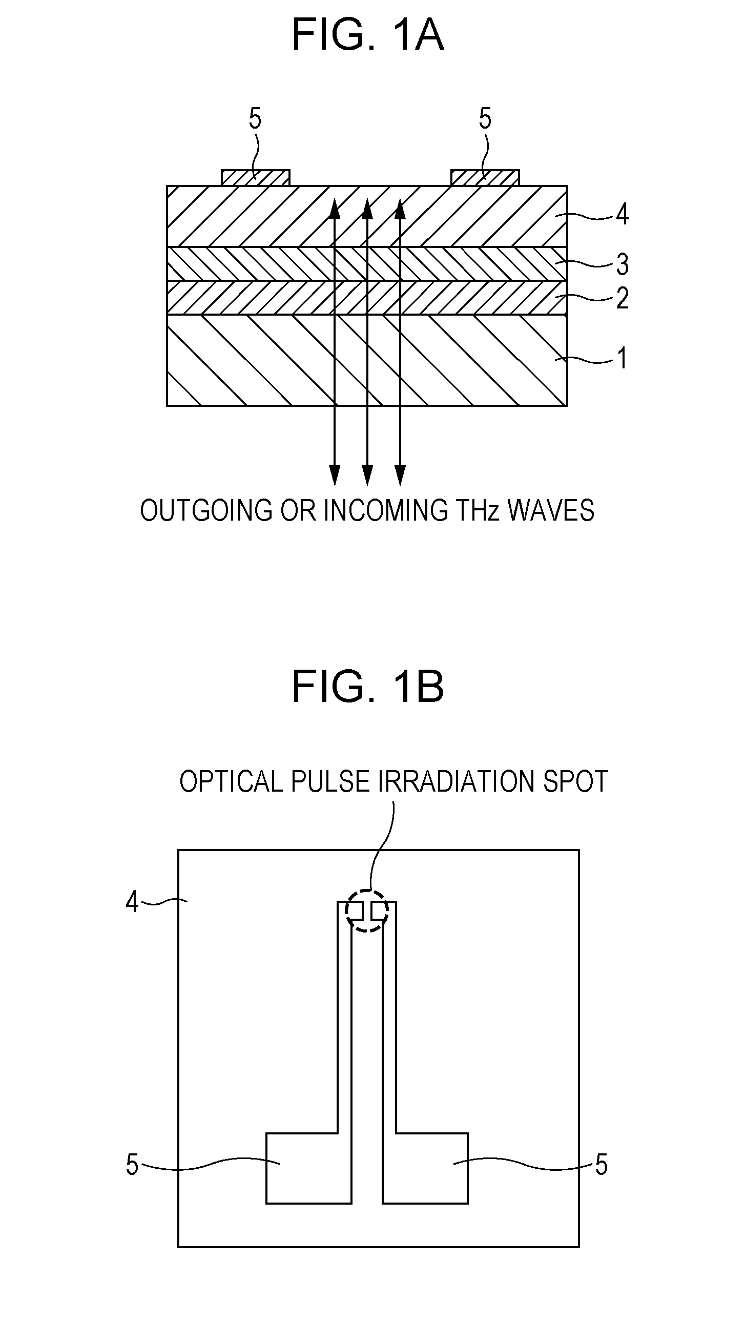
[0025]A first embodiment of the invention is described with reference to FIGS. 1A and 1B. FIGS. 1A and 1B are a cross-sectional view and a top view, respectively, of a photoconductive antenna according to this embodiment. FIGS. 1A and 1B illustrate a photoconductive antenna produced by growing crystals of Ge (a Ge layer) 2, GaAs (a first semiconductor layer that contains Ga and As) 3, and LT-GaAs (a second semiconductor layer that contains Ga and As) 4 on a Si substrate 1 in this order and then placing more than one electrode 5.

[0026]Low-resistivity silicon would lead to a great loss of THz waves due to absorption by free carriers. Thus the Si substrate 1 is made of semi-insulating Si, preferably having a resistivity of 10 Ω·cm or more. In this embodiment, silicon grown as a crystal with a resistivity of 3 kΩ·cm by the FZ process, which generally provides high-resistivity Si, is used as the Si substrate 1. The orientation of the substrate is (100), and substrates that have an off-an...

embodiment 2

[0038]Embodiment 2 is described. As illustrated in FIG. 3, this embodiment has a buffer layer 6, which is a thin film of Si(1-x)Ge, where x is a composition ratio, and has an increasing gradient of the composition ratio x in the direction of film growth, i.e., from the Si substrate 1 side to the GaAs 3 side. More specifically, the composition ratio x=0 at the end on the Si substrate 1 side, then x gradually changes, and x=1 at the end on the GaAs 3 side. The thin film of Si(1-x)Gex can be grown in the crystalline form by techniques such as reduced-pressure CVD (chemical vapor deposition) using monosilane (SiH4) and monogerman (GeH4). The composition ratio x can be controlled by the flow rates of the gases; gradually changing the flow rates of the gases leads to the composition ratio x gradually changing in the Si(1-x)Gex film.

[0039]The use of a thin film of Si(1-x)Gex as the buffer layer 6 provides a lattice constant gradient that extends from the Si substrate 1 to GaAs 3. As a resu...

embodiment 3

[0041]Embodiment 3 is described. As illustrated in FIG. 4, this embodiment has a current barrier layer 7 between GaAs 3 and LT-GaAs 4. The current barrier layer 7 can be, for example, a monolayer of AlxGa(1-x)As (0.5≦x≦1) or similar compound semiconductors or an alternate stack of AlxGa(1-x)As (0.5≦x≦1) and GaAs or similar combinations of compound semiconductors. This current barrier layer 7 can be grown in the crystalline form by techniques such as MBE (molecular beam epitaxy).

[0042]This current barrier layer 8 prevents the current that flows through LT-GaAs 4 between the electrodes 5 substantially parallel to the Si substrate 1 from flowing into the layers of GaAs 3 and Ge 2. This means that AlxGa(1-x)As in the current barrier layer 7 serves as an interband barrier and therefore should be about 10 nm thick to prevent tunnel currents. This also applies when the current barrier layer 7 is an alternate stack of AlxGa(1-x)As (0.5≦x≦1) and GaAs; each layer of AlxGa(1-x)As should be abo...


PUM


Abstract

A photoconductive antenna that generates and detects a terahertz wave has a substrate, a buffer layer, a first semiconductor layer, a second semiconductor layer, and an electrode in this order. The substrate is made of Si, the buffer layer contains Ge, and the first and second semiconductor layers both contain Ga and As. The element ratio Ga/As of the second semiconductor layer is smaller than the element ratio Ga/As of the first semiconductor layer.

Description

BACKGROUND OF THE INVENTION[0001]1. Field of the Invention[0002]The present invention relates to a photoconductive antenna, a method for producing a photoconductive antenna, and a terahertz time domain spectroscopy system.[0003]2. Description of the Related Art[0004]In recent years, nondestructive sensing technologies that use electromagnetic radiation from millimeter to terahertz (THz) waves (30 GHz to 30 THz, hereinafter also simply referred to as terahertz waves) have been developed. As a field of application of the electromagnetic radiation in this frequency band, an imaging technology as a means for fluoroscopic examinations safer than X-ray is under development. Spectroscopic technologies to characterize a substance, e.g., to identify the molecular bonding state, by determining the absorption spectrum and complex dielectric constant in the substance, measuring technologies to explore the carrier content, mobility, conductivity, and other characteristics, and analytical technol...

Claims


Application Information

Patent Timeline
IPC IPC(8): H01L31/0304H01L31/18
CPCH01L31/1844H01L31/03046H01L31/09H01L31/1852H01L21/02381H01L21/0245H01L21/02463H01L21/02502H01L21/02546H01L21/0262H01L21/02631H01Q9/285Y02E10/544
Inventor SATO, TAKAHIRO
Owner CANON KK
Why Eureka
Try Eureka