Microcavity carrier with image enhancement for laser ablation

a microcavity carrier and laser ablation technology, applied in the direction of layered product treatment, synthetic resin layered products, packaging, etc., can solve the problems of severe deformation of the resolution achievable by such a process, and achieve the effect of improving reproducibility, wide process windows, and improving release properties

Active Publication Date: 2014-09-18
POLAROID IP BV
View PDF2 Cites 9 Cited by
  • Summary
  • Abstract
  • Description
  • Claims
  • Application Information

AI Technical Summary

Benefits of technology

[0007]It has been observed that the microcavity arrays produced in certain embodiments of this invention provide significantly improved reproducibility and wider process windows both in the manufacturing of the microcavity carrier films and in the particle filling and transfer in the roll-to-roll manufacturing of fixed array ACFs as taught in the patent applications cited above and illustrated in FIG. 2. Significant improvements in both the filling efficiency (i.e., the percentage of particles captured by the microcavities) in the filling process and the release efficiency of the microcavity web or loop from the adhesive layer in the particle transfer process have been observed. While not to be bound by theory, it is believed that the sacrificial IEL effectively prevents debris and the low molecular weight laser-degraded or photolysis / thermolysis material melt from directly contacting or forming a strong adhesion / cohesion with the substrate. The low molecular weight laser-degraded or photolysis / thermolysis materials tend to be quite polar and sometimes charged. They tend to be quite sticky but were removed or washed away in the subsequent image development processes that dissolve or strip the IEL. As a result, the microcavity carrier webs or loops of this invention showed a significantly better release properties against the adhesive layer in the particle transfer process. On the other hand, the improvements observed in the particle filling process are believed to be the direct consequence of the better defined cavity partition and profile obtained using the IEL which may better contain the particles during the roll-to-roll fluidic particle filling process.
[0008]One manifestation of the invention is a carrier belt which comprises a substrate and a image enhancement layer (IEL) overcoating the substrate wherein the IEL is laser ablatable and prevents laser-degraded materials from interfering with formation of microcavities and enables the production of a microcavity carrier having fine pitch, high resolution and high aspect ratio.
[0010]Another manifestation of the invention is a carrier sheet, belt or web having an IEL in which the microcavities are arranged in a non-random but variable pattern to reduce the effect of periodic defects.

Problems solved by technology

For fine pitch image reproduction particularly those of high aspect ratio (i.e., the height / width or depth / width ratio of an image or image spacing), the resolution achievable by such a process is often severely degraded by the undesirable light diffraction and scattering attributable to the mask used and the aforementioned material melt flow, debris formation and re-deposition induced by the photothermal process.
However, in all cases, manufacturing of fine-pitch (about 1) of image spacing remains a major challenge, particularly in a roll-to-roll process.

Method used


Image

  • Microcavity carrier with image enhancement for laser ablation
  • Microcavity carrier with image enhancement for laser ablation
  • Microcavity carrier with image enhancement for laser ablation

Examples


Embodiment Construction

[0021]Liang '700 is incorporated herein, in its entirety, by reference.

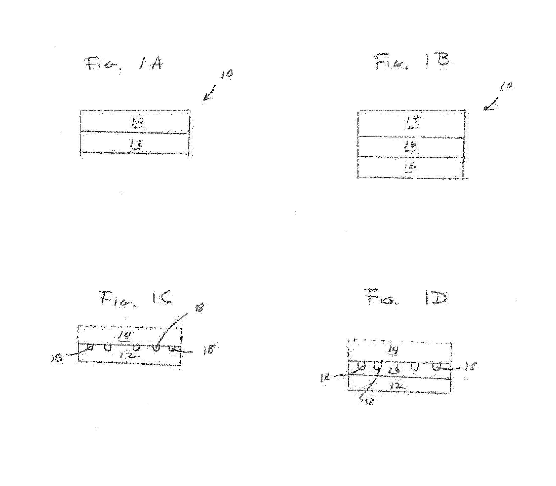
[0022]FIG. 1A is a cross-sectional view of a carrier sheet, web or belt 10 in accordance with one embodiment of the invention. The carrier sheet 10 includes a substrate 12 which is overcoated with a IEL 14 that may be directly bonded to the substrate 12. In another embodiment, as shown in FIG. 1B, the carrier 10 may optionally include an intermediate cavity-forming layer 16 which may be interposed between the IEL layer 14 and the substrate 12. In a particular embodiment the substrates 12 are formed by polyethylene terephthalate (PET), PEN, polyimide, etc., and the IEL 14 is a thin overcoat of an imaging enhancement sacrificial layer such as the PKFE and PKHB phenoxy resins (identified below). The microcavities are able to provide ultra-fine pitch and spacing

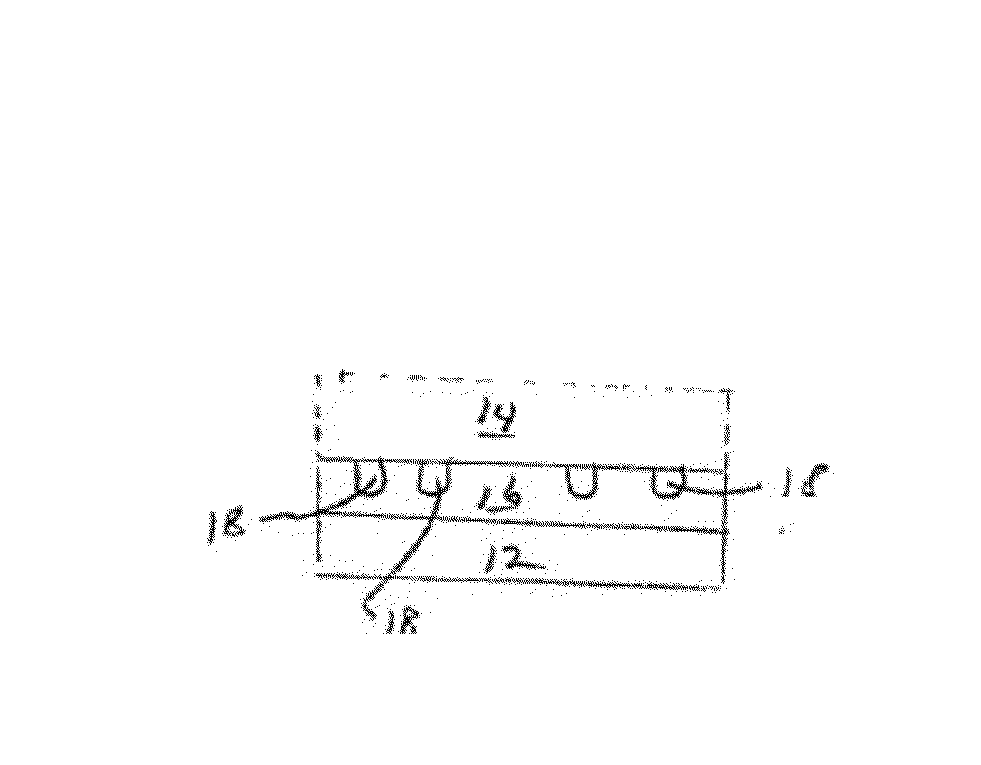
[0023]FIGS. 1C and 1D illustrate the carrier shown in FIG. 1A after formation of the microcavities 18 in the carrier 10 by laser ablation and after removal of...


PUM

PropertyMeasurementUnit
aspect ratioaaaaaaaaaa
diameteraaaaaaaaaa

Abstract

A carrier belt for fabricating a device or component such as an anisotropic conductive film. The carrier belt includes a substrate having a sacrificial image enhancing layer. Microcavities are formed in the carrier by laser ablation through the image enhancing layer. After the image enhancement layer is removed, a plurality of conductive particles are distributed into an array of microcavities formed by laser ablation on a surface of a carrier belt and transferred to an adhesive layer. The image enhancing layer enables one to form microcavities with a fine pitch and spacing and partitions having a high aspect ratio.

Description

FIELD OF INVENTION[0001]This invention relates to a method for manufacturing electronic devices and components such as anisotropic conductive films (ACF). This invention represents an improvement in the invention disclosed in U.S. Published Application 2010 / 0101700 to Liang et al. (“Liang '700”) in which an Image Enhancement Layer (IEL) is used to form the microcavities in the carrier web by laser ablation.BACKGROUND OF INVENTION[0002]For a discussion of the background of the invention reference may be made to Liang '700 cited above. Liang '700 discloses a method for manufacturing ACFs having a non-random array of conductive particles by providing a carrier web having a non-random array of microcavities and distributing the conductive particles into the microcavities. Preferably, the particles are distributed on the carrier web so that there is essentially one particle in each cavity. The carrier web is conveyed into contact with an adhesive film and the particles are transferred to...

Claims


Application Information

Patent Timeline
Patent Type & Authority Applications(United States)
IPC IPC(8): B32B37/00B32B38/00C08J7/043C08J7/044C08J7/046
CPCB32B37/0053B32B38/00B32B3/26H05K3/323B32B7/12B32B27/08B32B27/20B32B27/205B32B27/281B32B27/285B32B27/286B32B27/302B32B27/34B32B27/36B32B27/365B32B27/38B32B2255/10B32B2255/26B32B2264/0235B32B2264/025B32B2264/0257B32B2264/0264B32B2264/0292B32B2264/105B32B2270/00B32B2307/202B32B2307/714B32B2413/00B32B2310/0843Y10T428/31938Y10T428/31721Y10T428/31504Y10T428/31725Y10T428/31935Y10T428/24998Y10T428/249978Y10T428/31507Y10T428/31786Y10T428/31663Y10T428/31942B32B38/10C08J7/043C08J7/046C08J7/044
Inventor LIANG, RONG-CHANGTSENG, CHIN-JENWU, TA-CHINGLEONG, JIA YENAN, ZHIYAOMA, AN-YUAUNG, MAUNG KYAW
Owner POLAROID IP BV
Why Eureka
Try Eureka