

Photo-curable transfer sheet and method for forming concave-convex pattern using the same
a transfer sheet and concave technology, applied in the direction of electric heating, electrical/magnetic/electromagnetic heating, electrical equipment, etc., can solve the problems of high mold cost, high mold cost, and extremely difficult resin-sticking mold repair, etc., to achieve excellent mold release properties, low polarity, and excellent mold release properties
- Summary
- Abstract
- Description
- Claims
- Application Information
AI Technical Summary
Benefits of technology
Problems solved by technology
Method used
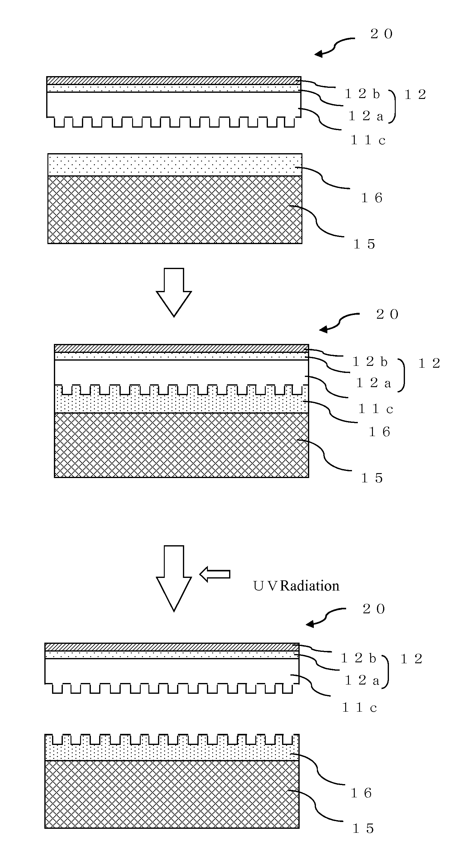
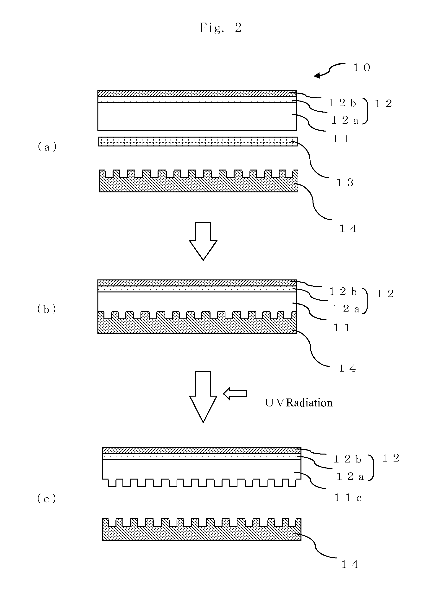
Image

Examples
example
(1) Preparation of Photo-Curable Composition
[0155]Monomers having composition ratio (molar ratio) shown in Table 1 were polymerized by known method to prepare polymers 1 to 6 having weight average molecular weight (Mw) and “alicyclic group containing monomer unit content rate P”=(“weight of alicyclic group containing monomer” / “total weight of all monomers”)×100(%) shown in Table 1. As monomers having an alicyclic group, isobornyl methacrylate (monomer C), cyclohexyl methacrylate (monomer D) and tetrahydrofurfuryl methacrylate (monomer E) were used.
TABLE 1Mixture ratioPolymerPolymerPolymerPolymerPolymerPolymer(molar ratio)123456Monomer A*1653133Monomer B*23—————Monomer C*3—468——Monomer D*4————6—Monomer E*5—————6Monomer F*6111111Weight average110,000 90,000 90,000 90,000 90,000 90,000 molecular weight(Mw)Alicyclic group058 76 89 70 70 containingmonomer unitcontent rate P*6(%)Note)*1Methyl methacrylate*2Butyl methacrylate*3Isobornyl methacrylate*4Cyclohexyl methacrylate*5Te...
examples 1 to 9
, and Comparison Examples 1 to 2
[0156]Photo-curable transfer sheets of Examples 1 to 9 and Comparison Examples 1 to 2 were prepared by using photo-curable compositions shown in Table 2.
TABLE 2(Photo-curable composition of photo-curable transfer layer)Exam-Exam-Exam-Exam-Exam-Exam-Exam-Exam-Exam-Co.Co.pleplepleplepleplepleplepleEx.Ex.Trade name12345678912PolymerPolymer-1—————————100 100 Polymer-2———————100 ———Polymer-3100 100 100 ——100 100 ————Polymer-4————————100 ——Polymer-5———100 ———————Polymer-6————100 ——————MonomerSR238F*8—100 100 100 100 70 130 100 100 100 —DCP-A*9100 —————————100 PhotoIrgacure2.02.02.02.02.01.72.32.02.02.02.0initiator651HardenerBXX56271.51.51.51.51.51.31.71.51.51.51.5InhibitorMEHQ 0.05 0.05 0.05 0.05 0.05 0.05 0.05 0.05 0.05 0.05 0.05InnerUV35002.02.02.02.02.01.72.32.02.02.02.0lubricantLTP-2——0.1————————Alicyclic group containing37.0 37.0 37.0 34.1 34.1 43.5 32.2 28.2 43.3 0 0 monomer unit content rate T*10Note)*81,6-hexane diol diacrylate...
PUM
| Property | Measurement | Unit |
|---|---|---|
| Tg | aaaaa | aaaaa |
| mol % | aaaaa | aaaaa |
| thickness | aaaaa | aaaaa |
Abstract
Description
Claims
Application Information