Methods for improving etching resistance for an amorphous carbon film

a technology of amorphous carbon film and etching resistance, which is applied in the field of process improvement and etching resistance improvement, can solve the problems of insufficient masking, insufficient pattern transfer accuracy, and complex devices of integrated circuits, and achieve the effect of high etching resistan

Inactive Publication Date: 2014-09-18
APPLIED MATERIALS INC
View PDF3 Cites 11 Cited by
  • Summary
  • Abstract
  • Description
  • Claims
  • Application Information

AI Technical Summary

Benefits of technology

[0009]Methods for using an electron beam treatment performed on an amorphous carbon layer to form a treated amorphous carbon layer with high etching resistance are provided. In one embodiment, a method of treating an amorphous carbon film includes providing a substrate having a material layer disposed, forming an amorphous carbon layer on the material layer, and performing an electron beam treatment process on the amorphous carbon layer.

Problems solved by technology

Integrated circuits have evolved into complex devices that can include millions of transistors, capacitors and resistors on a single chip.
As the geometry limits of the structures used to form semiconductor devices are pushed against technology limits, the need for accurate pattern transfer for the manufacture of structures having small critical dimensions and high aspect ratios has become increasingly difficult.
Such thin resist layers (e.g., less than about 2000 Å) can be insufficient to mask underlying material layers during the pattern transfer step due to attack by the chemical etchant.
After a long period of exposure to the aggressive etchants, the hardmask layer without sufficient etching resistance may be damaged, resulting in inaccurate pattern transfer and loss of dimensional control.
Additionally, stress in the deposited film and / or hardmask layer may also result in stress induced line edge bending and / or line breakage.

Method used


Image

  • Methods for improving etching resistance for an amorphous carbon film
  • Methods for improving etching resistance for an amorphous carbon film
  • Methods for improving etching resistance for an amorphous carbon film

Examples


Embodiment Construction

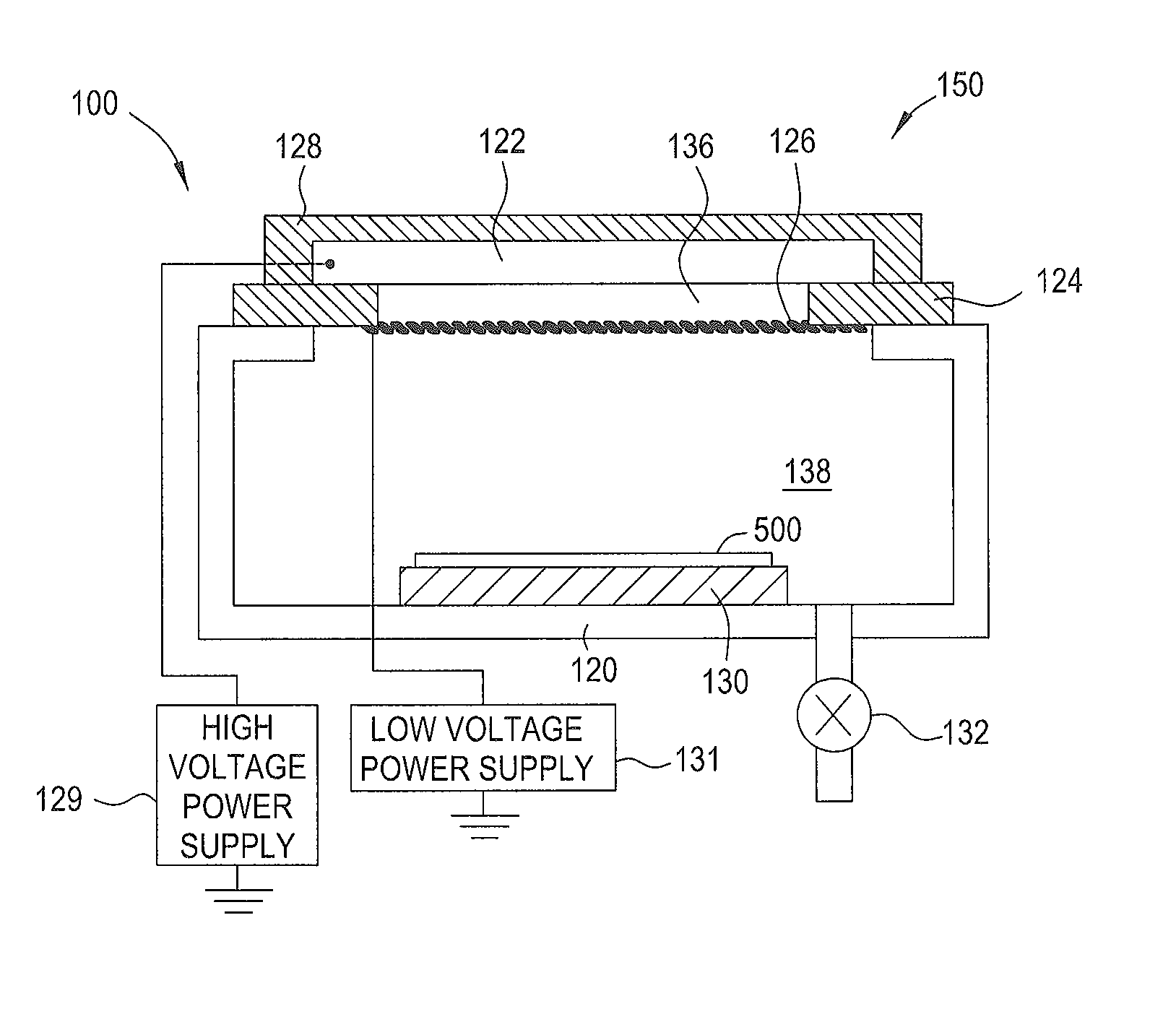
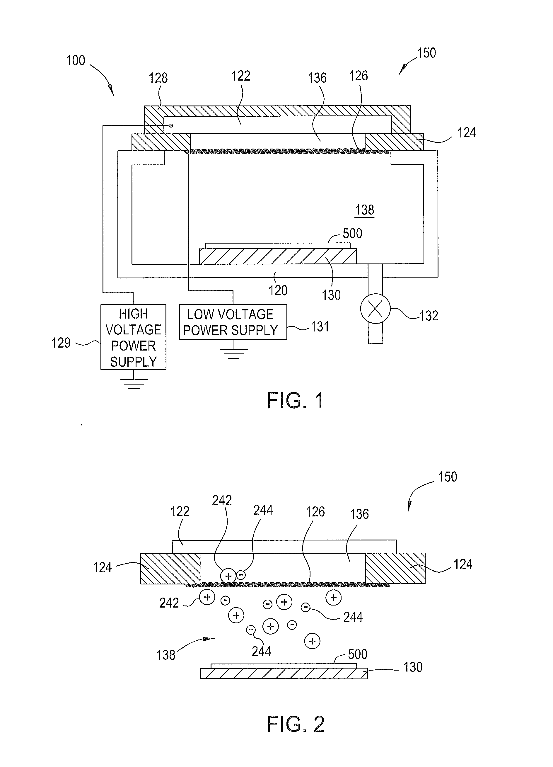
[0020]The present invention provides a method of performing an electron beam treatment process on an amorphous carbon layer to form a treated amorphous carbon layer with high etching resistance. In one embodiment, the amorphous carbon film is suitable for use as a hardmask layer. During the electron beam treatment process, the energy provided by the electron beam densifies the film structure of the amorphous carbon film, thereby producing the amorphous carbon layer with high density along with high etching resistance. The electron beam treated amorphous carbon film have desired mechanical properties, such as high density, hardness and suitable range of stress, which provides high film selectivity and etching resistance to other material layers for the subsequent etching process, thereby enabling good pattern transfer of small features to the underlying film stack with good profile control. Additionally, the electron beam treated amorphous carbon film also provides desired optical fi...


PUM

PropertyMeasurementUnit
currentaaaaaaaaaa
currentaaaaaaaaaa
bias voltageaaaaaaaaaa

Abstract

Methods for using an electron beam treatment performed on an amorphous carbon layer to form a treated amorphous carbon layer with high etching resistance are provided. In one embodiment, a method of treating an amorphous carbon film includes providing a substrate having a material layer disposed, forming an amorphous carbon layer on the material layer, and performing an electron beam treatment process on the amorphous carbon layer.

Description

CROSS-REFERENCE TO RELATED APPLICATION[0001]This application claims benefit of U.S. Provisional Application Ser. No. 61 / 787,071 filed Mar. 15, 2013 (Attorney Docket No. APPM / 17402L), which is incorporated by reference in its entirety.BACKGROUND[0002]1. Field of the Invention[0003]The present invention relates to the fabrication of integrated circuits and to a process for forming materials with high etching resistance on a substrate. More specifically, the invention relates to a process for improving etching resistance for a carbon containing material for semiconductor applications.[0004]2. Description of the Background Art[0005]Integrated circuits have evolved into complex devices that can include millions of transistors, capacitors and resistors on a single chip. The evolution of chip designs continually requires faster circuitry and greater circuit density. The demands for faster circuits with greater circuit densities impose corresponding demands on the materials used to fabricat...

Claims


Application Information

Patent Timeline
Patent Type & Authority Applications(United States)
IPC IPC(8): B05D3/06H01J37/30
CPCH01J37/3007B05D3/06C23C16/26C23C16/56H01J37/32422H01L21/02115H01L21/02274H01L21/02351H01L21/0332H01L21/0337H01L21/31122
Inventor ROSSLEE, CRAIGNEMANI, SRINIVAS D.LUBOMIRSKY, DMITRYYIEH, ELLIE Y.
Owner APPLIED MATERIALS INC
Why Eureka
Try Eureka