
Fluorine Passivation in CMOS Image Sensors

a technology of fluorine passivation and image sensor, which is applied in the direction of radiation control device, semiconductor/solid-state device testing/measurement, transistor, etc., can solve the problems of limited signal to noise ratio (snr), insufficient reduction, and reduced dark current in the cis. achieve the effect of reducing the dark current in the cis

Inactive Publication Date: 2014-09-18
INTERMOLECULAR
View PDF8 Cites 84 Cited by
  • Summary
  • Abstract
  • Description
  • Claims
  • Application Information

AI Technical Summary

Benefits of technology

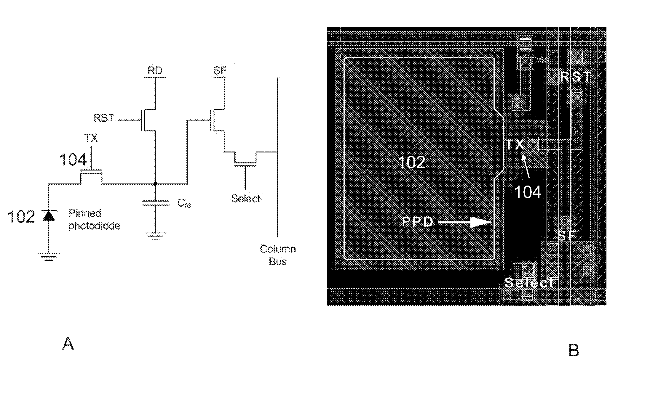
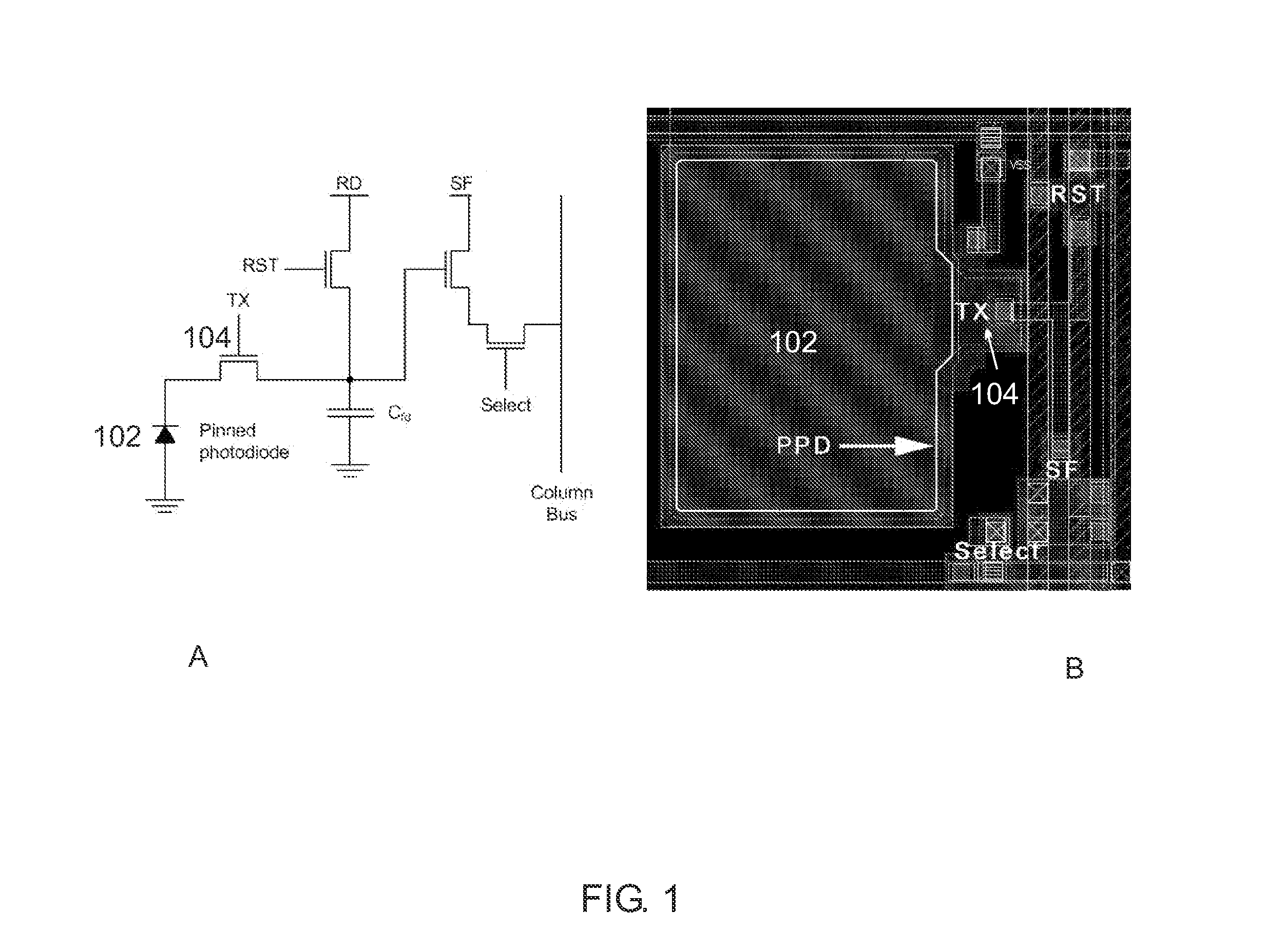
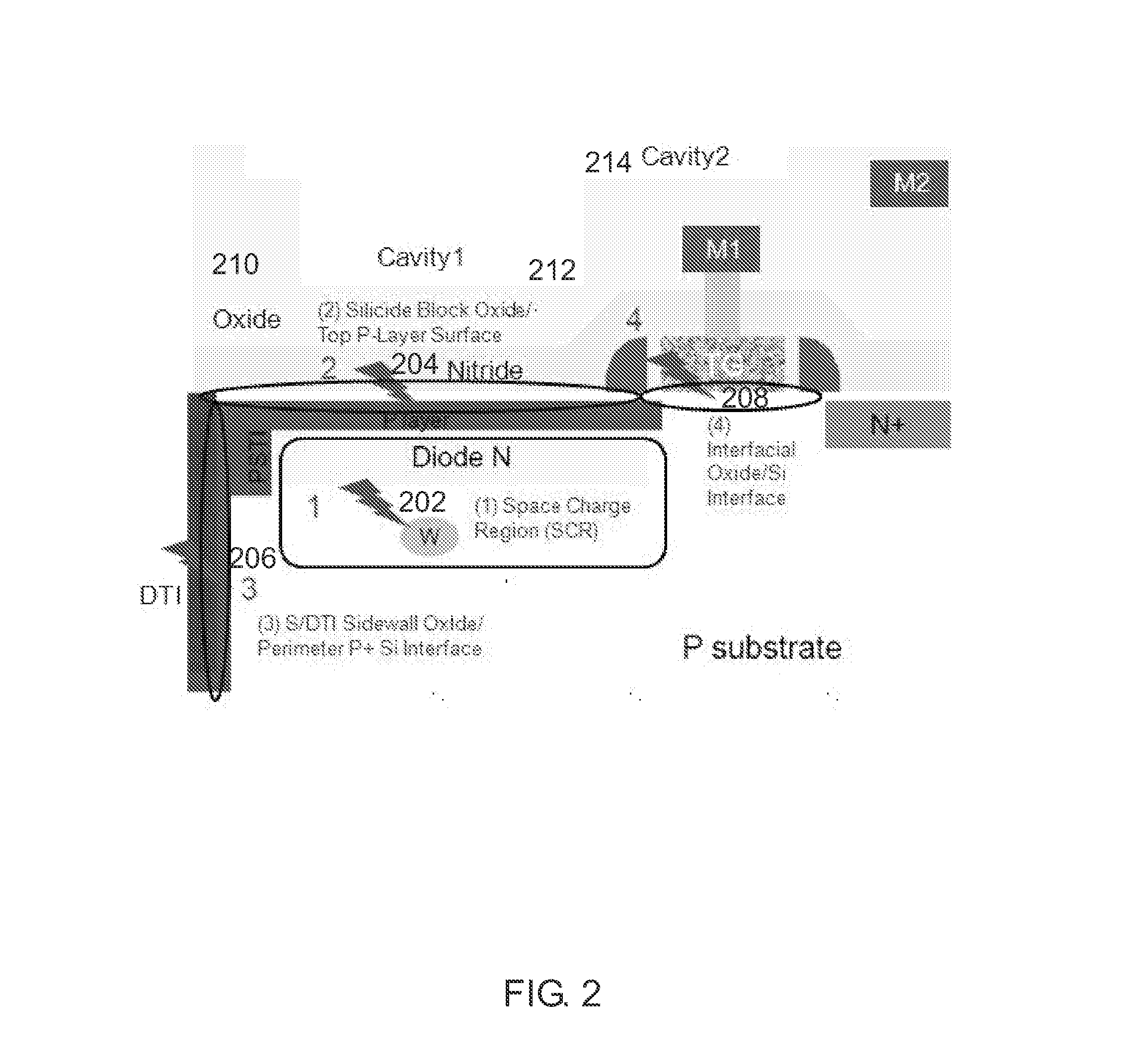
The present invention offers methods of making a fluorine-passivated CMOS imaging sensor (CIS) and a CIS that includes fluorine atoms in certain regions of the CIS. The fluorine atoms serve to passivate dangling Si atoms in the CIS, reducing dark current. The methods involve annealing the CIS in the presence of a source of fluorine atoms, such as F2, NF3, or CF4, or depositing a fluorine-containing SiO2 layer or fluorinated silicate glass layer on the CIS. The CIS comprises a pinned photodiode, an isolation trench, and a plurality of transistors, and at least one region of the CIS, such as the pinned photodiode, isolation trench, or transistors, is fluorine-passivated. The technical effects of the present invention are reduced dark current and improved performance of the CIS.

Problems solved by technology

As the pixel size is scaled for higher image resolution and / or higher density of integration in advanced CMOS image sensor (CIS) technology, dark current reduction is one of the main problems that limits signal to noise ratio (SNR).
Hydrogen (H2) passivation is commonly used to reduce the dark current, although the reduction may be insufficient as the pixel size is reduced.
However, the ion implantation process can create additional defects requiring subsequent thermal annealing steps at the high temperature to reduce the additional defects.

Method used


Image

  • Fluorine Passivation in CMOS Image Sensors
  • Fluorine Passivation in CMOS Image Sensors
  • Fluorine Passivation in CMOS Image Sensors

Examples


Embodiment Construction

[0021]It is to be understood that the terminology used herein is for the purpose of describing particular embodiments only and is not intended to limit the scope of the present invention.

[0022]It must be noted that as used herein and in the claims, the singular forms “a,”“an,” and “the” include plural referents unless the context clearly dictates otherwise. Thus, for example, reference to “a layer” includes two or more layers, and so forth.

[0023]Where a range of values is provided, it is understood that each intervening value, to the tenth of the unit of the lower limit unless the context clearly dictates otherwise, between the upper and lower limits of that range, and any other stated or intervening value in that stated range, is encompassed within the invention. The upper and lower limits of these smaller ranges may independently be included in the smaller ranges, and are also encompassed within the invention, subject to any specifically excluded limit in the stated range. Where t...


PUM


Abstract

CMOS imaging sensors having fluorine-passivated structures to reduce dark current are disclosed together with methods of making thereof. The CIS comprises an array of pixels on a substrate, each pixel comprising a pinned photodiode, an isolation trench adjacent to the pinned photodiode, and a plurality of transistors. Methods of preparing a CIS comprise providing a source of fluorine (F) atoms, and annealing in the presence of the source of F atoms. After the annealing, at least one silicon-containing surface or region in the CIS comprises Si—F bonds and is fluorine passivated.

Description

CROSS-REFERENCE TO RELATED APPLICATION[0001]This application claims priority from U.S. Provisional Patent Application No. 61 / 779,740, filed on Mar. 13, 2013, which is incorporated by reference herein in its entirety for all purposes.FIELD OF THE INVENTION[0002]One or more embodiments of the present invention relate to CMOS image sensors and methods of making thereof.BACKGROUND[0003]As the pixel size is scaled for higher image resolution and / or higher density of integration in advanced CMOS image sensor (CIS) technology, dark current reduction is one of the main problems that limits signal to noise ratio (SNR). The dark current comes from several sources, including minority carrier diffusion current in the photodiode, surface recombination centers and / or traps (Nst) at the trench sidewall liner and the top p-layer interfaces in contact with bulk silicon, the transfer gate interfacial SiO2 / Si interface (Dit), and bulk metallic contamination sites (Cu, Mo, Au, etc.) in the silicon with...

Claims


Application Information

Patent Timeline
Patent Type & Authority Applications(United States)
IPC IPC(8): H01L27/146
CPCH01L27/1462H01L27/14643H01L27/14698H01L29/778H01L29/1606H01L29/66742H01L29/786H01L29/66477H01L21/28575H01L21/02172H01L21/02175H01L21/283H01L29/41H01L21/02005H01L21/02104H01L21/3065H01L21/02178H01L21/02181H01L21/02189H01L21/02205H01L21/0228H01L21/76864H01L22/12H01L22/14
Inventor LEE, MANKOOBARABASH, SERGEYCHIANG, TONY P.PRAMANIK, DIPANKAR
Owner INTERMOLECULAR
Learn More