Micromachined High Breakdown Voltage ESD Protection Device for Light Emitting Diode and Method of Making the Same

a technology of esd protection device and light emitting diode, which is applied in the direction of emergency protective arrangement for limiting excess voltage/current, semiconductor device, electrical apparatus, etc., can solve the problems of silicon nitride, uniformity and cost, and the inside of the dielectric film can greatly reduce the nominal breakdown voltage so as to prolong the life of the dielectric film and high breakdown voltage protection

Inactive Publication Date: 2014-09-18
WISENSTECH
View PDF5 Cites 10 Cited by
  • Summary
  • Abstract
  • Description
  • Claims
  • Application Information

AI Technical Summary

Benefits of technology

[0007]It is therefore an object of the present invention to resolve the above issues of prior conventional arts. The objective of this invention is to provide a high breakdown voltage ESD protection for LEDs, which can prevent the LEDs from burning down and extends their lifespan. The LED chip is engaged to a parallel connection with a RC circuit which is microfabricated by micro-electro-mechanic system (a.k.a. MEMS) technology. Because the breakdown voltage of thin film is equal to the breakdown strength times the thickness of the thin film, therefore, one embodiment of the current invention, is to utilize thick polyimide layer as its dielectric layer between the top and bottom electrodes for the capacitor for the ESD protection device. By deploying this embodiment, the capacitor in current invention, can provide one order higher of breakdown voltage compared to the other type of capacitor due to its great thickness of dielectric layer.

Problems solved by technology

On the other hand, it would be very challenging for silicon nitride, silicon dioxide to deposit a layer with more than 3 um in thickness, wherein the challenges may come from the issues of high stress, uniformity and cost.
The defects inside the dielectric film can greatly reduce its nominal breakdown voltage.

Method used


Image

  • Micromachined High Breakdown Voltage ESD Protection Device for Light Emitting Diode and Method of Making the Same
  • Micromachined High Breakdown Voltage ESD Protection Device for Light Emitting Diode and Method of Making the Same
  • Micromachined High Breakdown Voltage ESD Protection Device for Light Emitting Diode and Method of Making the Same

Examples


Embodiment Construction

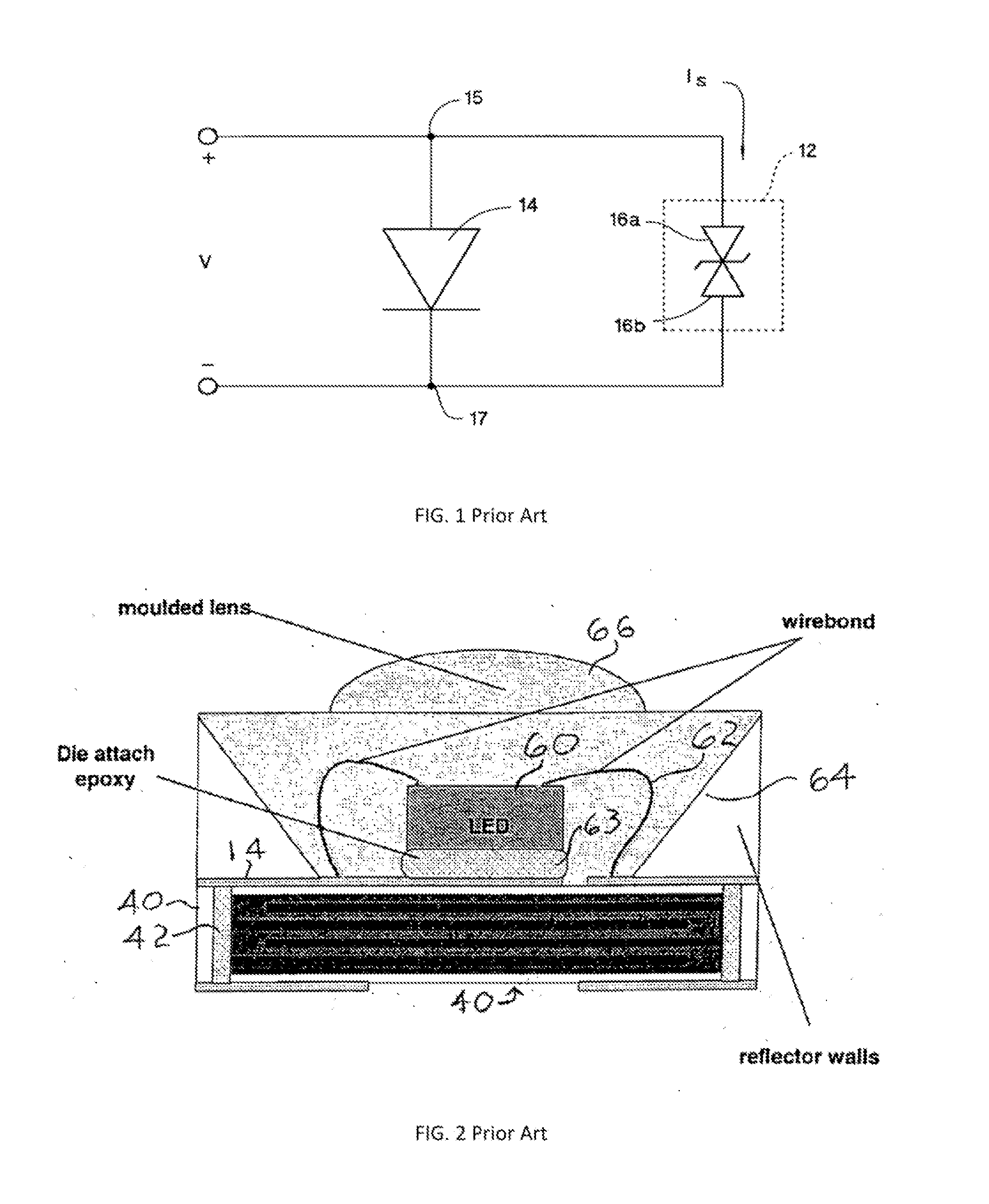
[0017]FIG. 1 and FIG. 2 are two prior arts of the ESD protection methods.

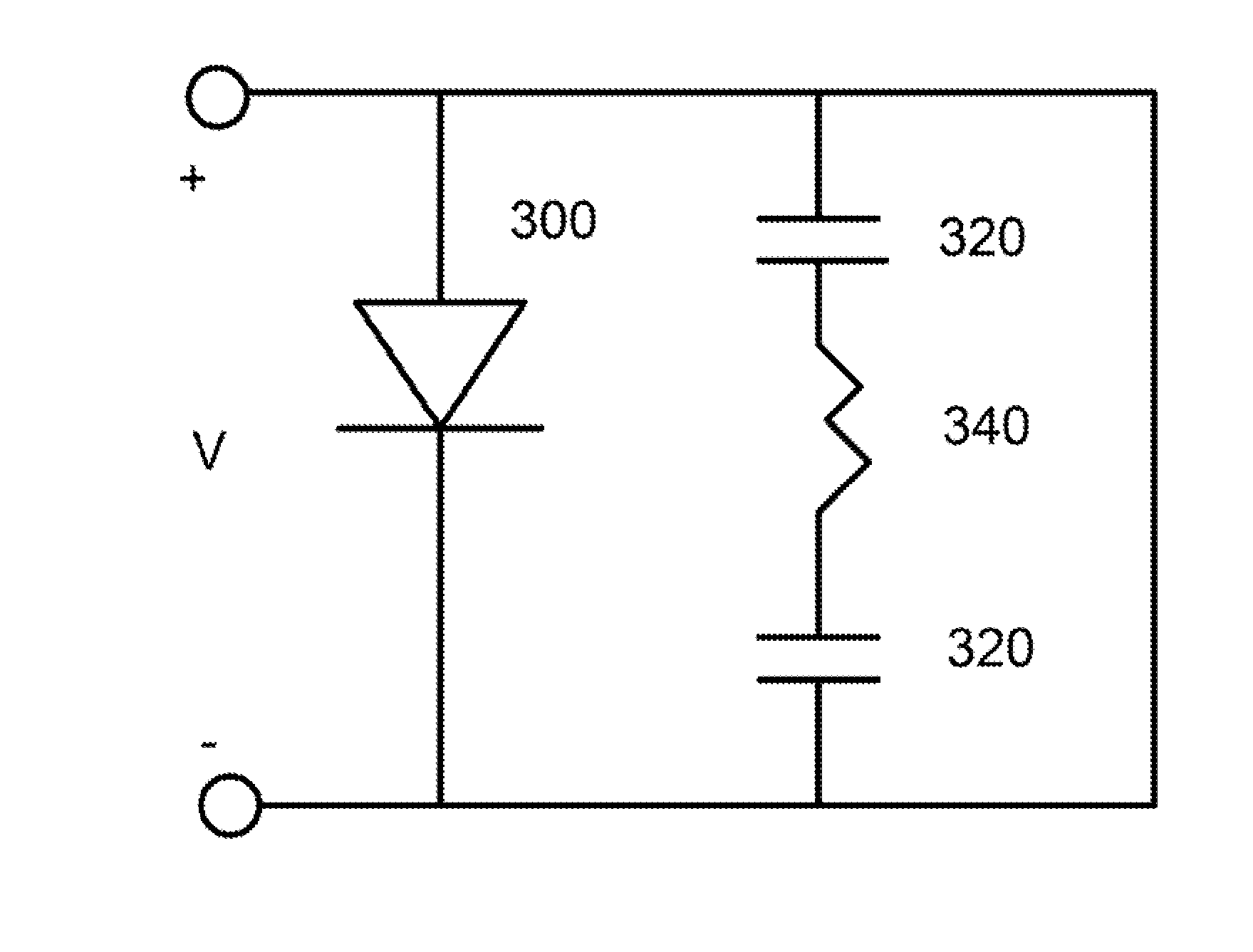
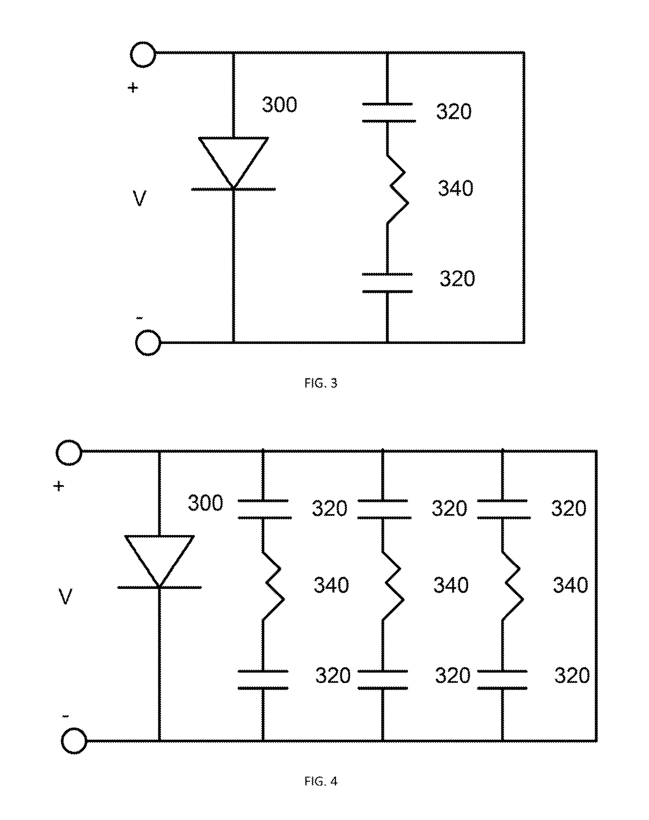
[0018]FIG. 3 illustrates a schematic of the preferred topology for the current invention. A micromachined ESD protection device is separately fabricated and integrated with the LED chip. The configuration of the ESD protection device comprises two identical capacitors 320 and one resistor 340. The resistor is disposed between the two identical capacitors. The ESD protection device in the current invention is connected to the LED chip 300 in a shunt connection to absorb and eliminate the voltage spike or electro static charges generated from the human contacts. Because the two capacitors are identical, therefore ESD protection device would be symmetrical and functional for the LED chip no matter the voltage spike is coming from which direction.

[0019]FIG. 4 shows another preferred embodiment of the current invention. An ESD protection array is formed by connecting three single ESD protection device of the current...


PUM


Abstract

This invention relates to a micromachined ESD protection device and its microfabrication method for light emitting diode (LEDs) chips. The LEDs is coupled to the ESD protection device in a shunt connection to absorb and eliminate the electrostatic charges induced by human contact or other voltage spike sources. The ESD protection circuit can prevent the LED from burning down and extend its lifespan. By using a thick polyimide layer as the dielectric film for capacitors in the micromachined ESD protection device at the current invention has the advantages with high breakdown voltage compared to other ESD protection circuits. And furthermore, the device in the current invention is easy for mass production with low manufacturing cost. Another embodiment of the present invention is that the multiple-array arrangement in current micromachined ESD protection device could greatly enhance the liability due to multiple-protection and thus to provide the possibility of multiple-times usage.

Description

BACKGROUND OF THE INVENTION[0001]1. Field of the Invention[0002]This invention relates to a micromachined ESD protection device for light emitting diodes (LED) chips and its micro-fabricating method. The LED chip is coupled with the invented ESD protection device in a shunt connection on a same mounted substrate to absorb and eliminate the electrostatic charges which are induced by voltage spike sources such as human contacts and thus to prevent the LED from burning down and extend its lifespan.[0003]2. Description of the Related Art[0004]In view of the current trend of development, it is fully expected that the brightness of the LED chips will serve as a highly efficient light source in the near future. Due to the superb characteristics of low power consumption, high luminous efficiency and long lifespan of light emitting diodes (LEDs) compared to other conventional light sources, the LEDs lighting for domestic and commercial applications are becoming prevailed and steadily penetra...

Claims


Application Information

Patent Timeline
Patent Type & Authority Applications(United States)
IPC IPC(8): H02H9/04
CPCH02H9/04H01L27/0248H02H9/046
Inventor CHEN, CHIH-CHANGHUANG, LIJI
Owner WISENSTECH
Why Eureka
Try Eureka