Method of reducion graphene oxide and reduced graphene oxide obtained by the method, and thin film transistor including the reduced graphene oxide

Inactive Publication Date: 2014-09-25
KOREA INST OF SCI & TECH
View PDF8 Cites 14 Cited by
  • Summary
  • Abstract
  • Description
  • Claims
  • Application Information

AI Technical Summary

Benefits of technology

[0031]An environmentally friendly, fast, and simplified method of reducing a graphene oxide without using a chemical solution such as a reducing agent and without a separate p

Problems solved by technology

However, as the indium tin oxide becomes expensive due to increasing consumption of indium, economy may be deteriorated, and in particular, since the transparent conductive layer including the indium has a chemical and electrical defect, an alternative tra

Method used


Image

  • Method of reducion graphene oxide and reduced graphene oxide obtained by the method, and thin film transistor including the reduced graphene oxide
  • Method of reducion graphene oxide and reduced graphene oxide obtained by the method, and thin film transistor including the reduced graphene oxide
  • Method of reducion graphene oxide and reduced graphene oxide obtained by the method, and thin film transistor including the reduced graphene oxide

Examples


Example

EXAMPLE 1

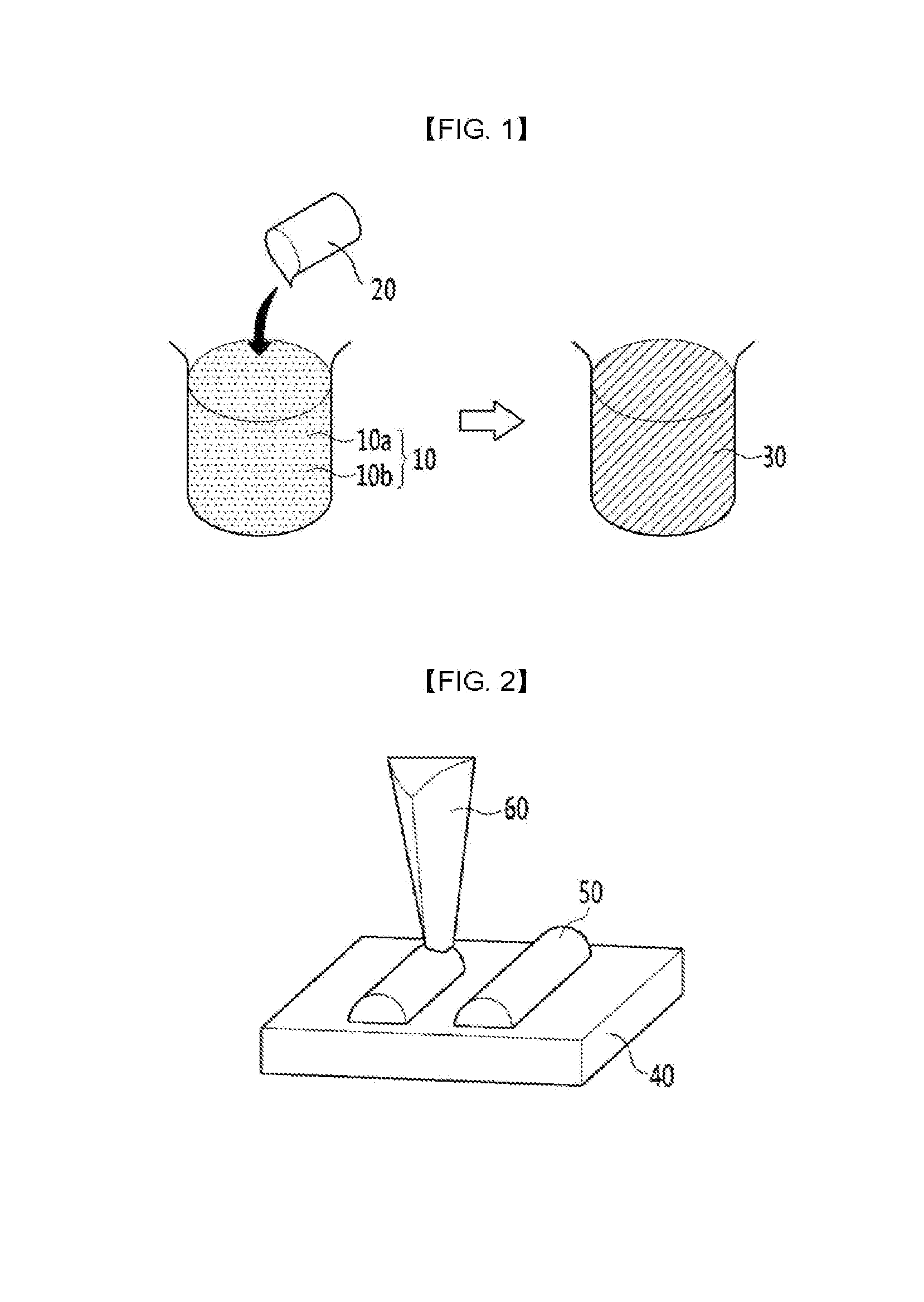
Preparation of Graphene Oxide Solution

[0079]25 mg of graphene oxide is obtained by oxidizing 1 g of graphite powder (Sigma Aldrich Co., Ltd.) with 5 g of potassium permanganate (KMnO4). Subsequently, 50 mg of the graphene oxide is added to 3 ml of water and the mixture is ultrasonicated, preparing a graphene oxide dispersion. Thereafter, 6 mL of n-methylpyrrolidone (NMP) is added to the graphene oxide dispersion and the mixture is agitated, preparing a graphene oxide solution.

Formation of Reduced Graphene Oxide Pattern

[0080]The graphene oxide solution is then deposited in a dropwise fashion on a silicon wafer with a microfluidic dispenser to print a plurality of graphene oxide patterns having a width of 120 μm. Subsequently, the silicon wafer is disposed inside a globe box, and reduced graphene oxide patterns are formed by radiating 50 white light pulses with an energy amount of 60 J / cm2 for 6 ms of on-time and 5 ms of off-time on the graphene oxide patterns.

Example

EXAMPLE 2

[0081]A reduced graphene oxide pattern is formed under the same conditions as in Example 1, except for changing the number of radiation shots of the white light pulse to two, three, five, ten, and twenty.

Evaluation 1

[0082]The reduced graphene oxide pattern of Example 1 is analyzed by using x-ray photoelectron spectroscopy (XPS).

[0083]FIG. 5 (a) is an XPS graph showing the graphene oxide before radiation of the white light pulse, and FIG. 5 (b) is an XPS graph showing the reduced graphene oxide after radiation of the white light pulse.

[0084]Referring to FIG. 5, the graphene oxide before radiation of the white light pulse shows peaks of bonding energy (C—C) of about 284.7 eV, bonding energy (C—O) of about 286.2 eV, bonding energy (C═O) of about 287.8 eV, and bonding energy (C(O)O) of 289.0 eV, but the reduced graphene oxide after radiation of the white light pulse shows only a peak of bonding energy (C—C) of about 284.7 eV.

[0085]Accordingly, the graphene oxide is reduced by ...

Example

EXAMPLE 3

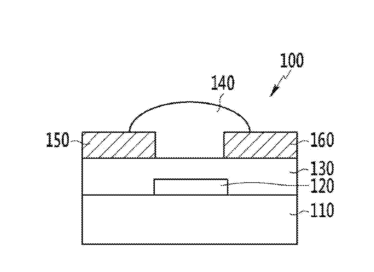
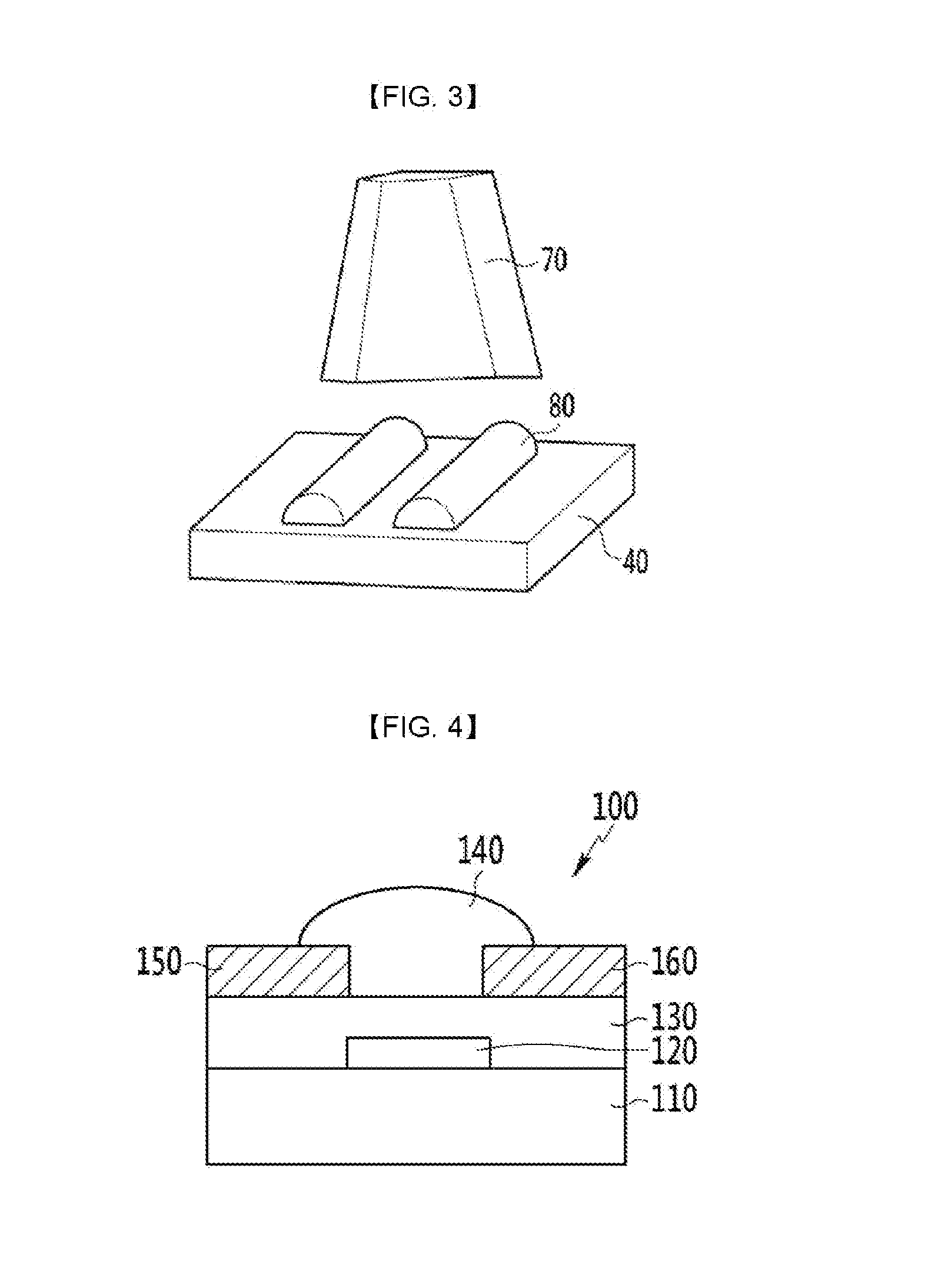
Manufacture of Thin Film Transistor 1

[0093]Silicon oxide (SiO2) is deposited to be 300 nm thick on a silicon substrate doped in a high concentration. The graphene oxide solution according to Example 1 is deposited at a predetermined interval with a microfluidic dispenser to form a graphene oxide pattern. Subsequently, the graphene oxide pattern is radiated by 50 pulses of a white light pulse for an on-time of 6 ms and an off-time of 5 ms with an energy amount of 60 J / cm2, forming source and drain electrodes formed of the reduced graphene oxide. Poly(3-hexylthiophene) (P3HT) is then inkjet-printed on the source and drain electrodes and dried, manufacturing a thin film transistor.

Evaluation 4

[0094]Current characteristics of the thin film transistor according to Example 3 are evaluated.

[0095]FIG. 9 is a graph showing current characteristics (IDS-VDS) of the thin film transistor according to Example 3.

[0096]Referring to FIG. 9, the thin film transistor according to Example 3 ha...


PUM

PropertyMeasurementUnit
Timeaaaaaaaaaa
Timeaaaaaaaaaa
Timeaaaaaaaaaa

Abstract

Disclosed are a method of manufacturing a reduced graphene oxide pattern which includes forming a graphene oxide pattern on a substrate and providing the graphene oxide pattern with a white light pulse to reduce the graphene oxide, a reduced graphene oxide obtained by the method, and an electronic device and a thin film transistor including the reduced graphene oxide.

Description

[0001]This application claims priority to and the benefit of Korean Patent Application No. 10-2013-0029983 filed in the Korean Intellectual Property Office on Mar. 20, 2013, the entire contents of which are incorporated herein by reference.BACKGROUND OF THE INVENTION[0002](a) Field of the Invention[0003]A method of manufacturing a reducing graphene oxide, a reduced graphene oxide obtained by the method, and a thin film transistor including the reduced graphene oxide are disclosed.[0004](b) Description of the Related Art[0005]In general, various electronic devices such as a display device, a light emitting diode, a solar cell, and the like form an image or generate electricity by transmitting light, and thus necessarily require a transparent conductive layer being capable of transmitting light. Indium tin oxide (ITO) has been widely used to form such a transparent conductive layer.[0006]However, as the indium tin oxide becomes expensive due to increasing consumption of indium, econom...

Claims


Application Information

Patent Timeline
IPC IPC(8): H01L29/49H01L29/786C01B31/04
CPCH01L29/4908H01L29/786C01B31/043C01B32/192H01L21/0237H01L21/02527H01L21/02601H01L21/02628H01L21/02664H01L29/1606H01L29/401H01L29/41725H01L29/41733H01L29/458H01L29/66477Y10T428/24802B82B1/008B82B3/0095C01B32/23
Inventor LIM, JUNG AHSONG, YONG-WONHONG, JAE-MINCHANG, JOO YOUNG
Owner KOREA INST OF SCI & TECH
Why Eureka
Try Eureka