Semiconductor device and high side circuit drive method

Active Publication Date: 2014-10-02
FUJI ELECTRIC CO LTD
View PDF2 Cites 12 Cited by
  • Summary
  • Abstract
  • Description
  • Claims
  • Application Information

AI Technical Summary

Benefits of technology

[0033]As heretofore described, according to the invention, it is possible to suppress a delay when there is dead time, or the like, in an operation of turning on a high potential side

Problems solved by technology

Because of this, power loss due to the diode DH connected

Method used


Image

  • Semiconductor device and high side circuit drive method
  • Semiconductor device and high side circuit drive method
  • Semiconductor device and high side circuit drive method

Examples


first embodiment

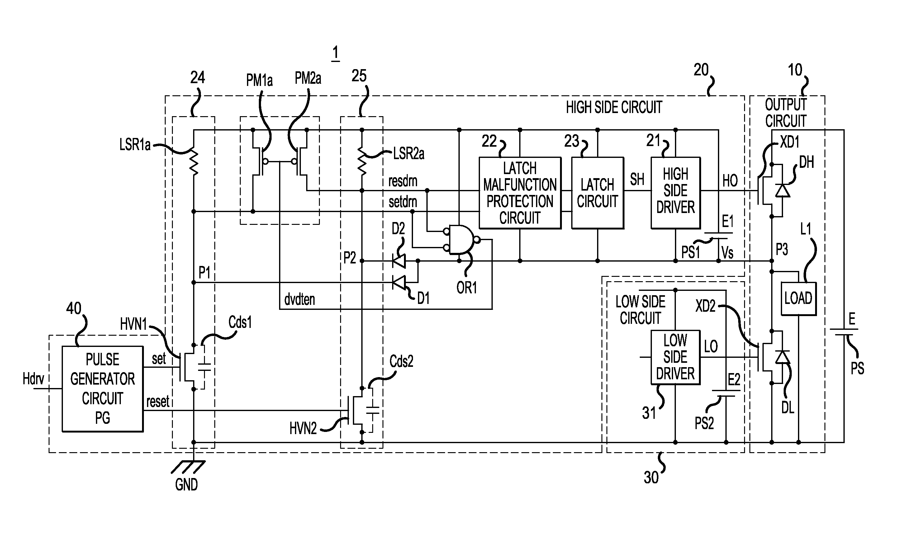
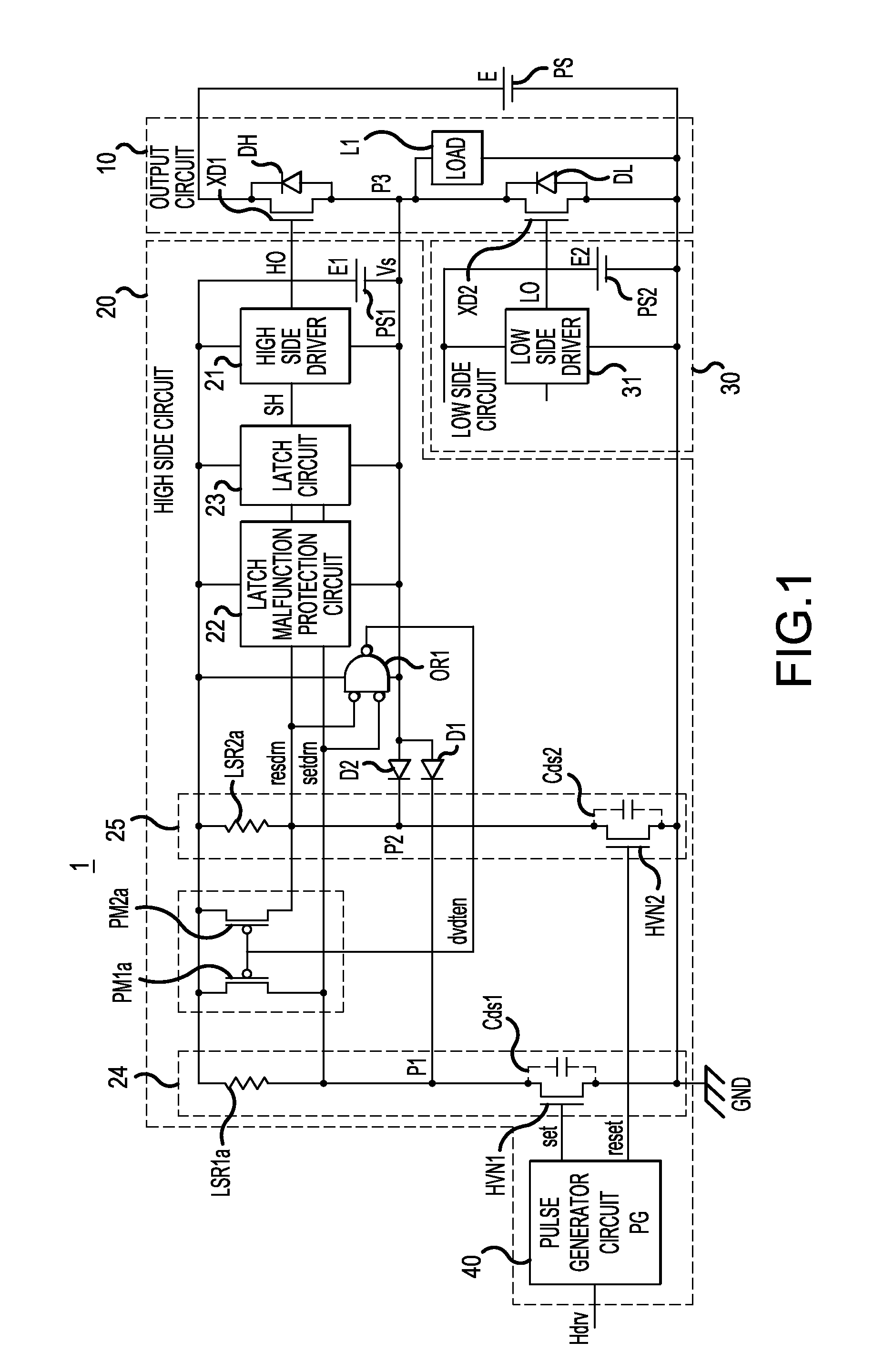
[0047]FIG. 1 shows a configuration of a half-bridge drive circuit as one example of a semiconductor device according to the invention. A half-bridge drive circuit 1 is configured of a high side circuit 20 and a low side circuit 30. However as the invention relates to the high side circuit 20, and the relationship thereof with the low side circuit 30 is weak, a description of the low side circuit 30 will be abbreviated.

[0048]In FIG. 1, an output circuit 10 includes switching elements XD1 and XD2 connected in a totem pole configuring a half-bridge, and an output voltage E of a high voltage power supply PS is applied to either end thereof. For example, an n-type channel or p-type channel MOS transistor, a p-type or n-type IGBT, or the like, is used for the high potential side (high side) switching element XD1. For example, an n-type channel MOS transistor, an n-type IGBT, or the like, is used for the low potential side (low side) switching element XD2. Herein, n-type channel MOS transi...

second embodiment

[0078]Next, a description will be given of a second embodiment of the invention.

[0079]FIG. 3 shows a configuration of a half-bridge drive circuit including a high side circuit according to this embodiment. A difference from FIG. 1 is that p-type channel MOS transistors PM1 and PM2, resistors LSR1b and LSR2b, and a NOT circuit 26 have been added. As the remainder is the same as FIG. 1, the same reference signs are given to the same components, and a description will be omitted.

[0080]The MOS transistors PM1 and PM2 are connected in parallel to the resistors LSR1a and LSR2a respectively, and the gate terminals thereof are connected to the connection points P2 and P1 respectively.

[0081]One end of the resistor LSR1b is connected to the connection point P1, while the other end is connected to the output terminal of the NOT circuit 26. Also, one end of the resistor LSR2b is connected to the connection point P2, while the other end is connected to the output terminal of the latch circuit 23...

third embodiment

[0098]Next, a description will be given of a third embodiment of the invention.

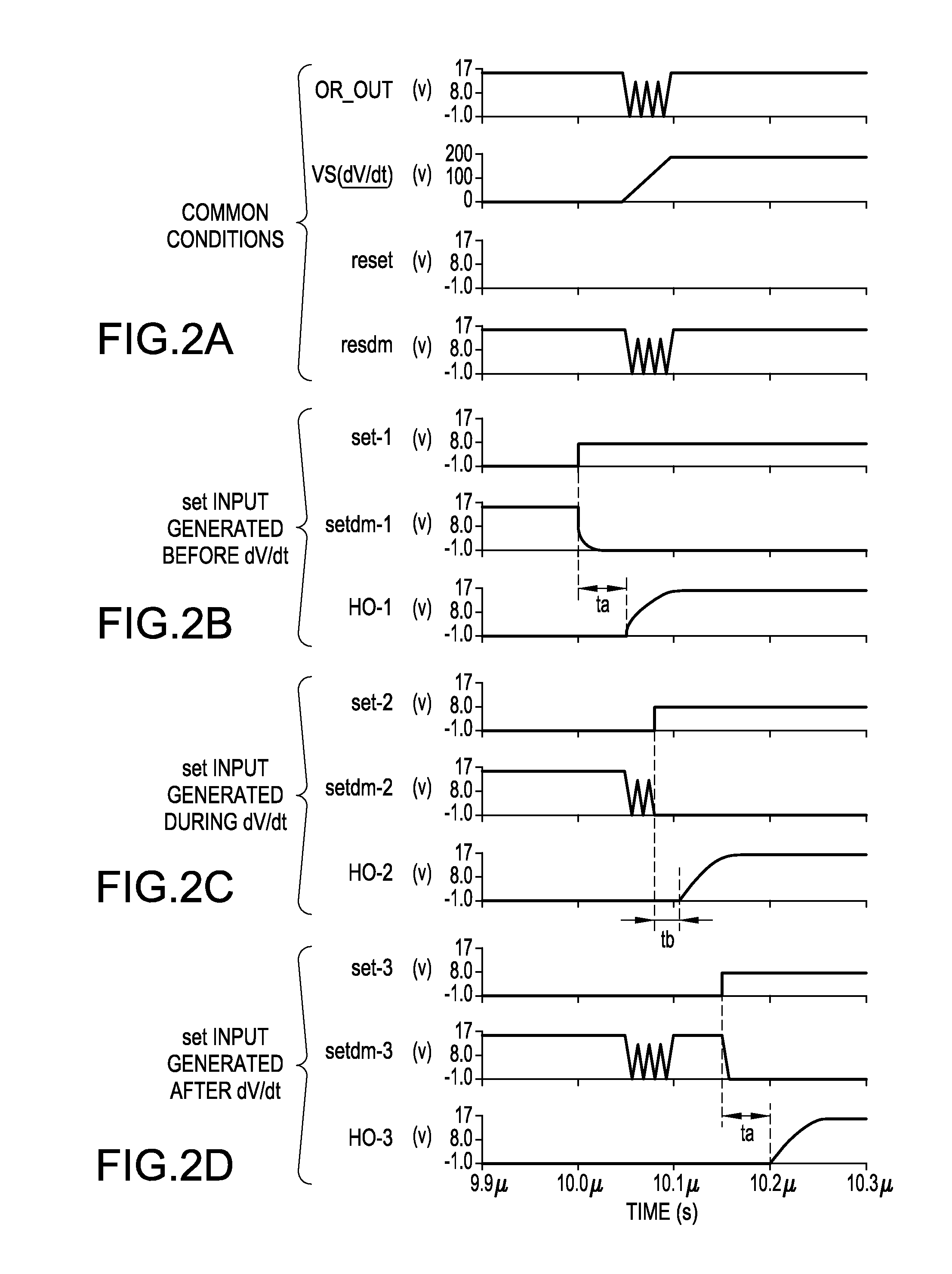
[0099]The half bridge drive circuit 1 according to this embodiment is such that a signal with an output waveform different from that heretofore known is output from the pulse generator circuit 40 in the high side circuit 20 shown in FIG. 1 and FIG. 3.

[0100]FIG. 4 is a circuit configuration diagram of the pulse generator circuit 40 according to this embodiment. In FIG. 4, the input signal Hdrv from the exterior is input into a D input terminal of a D-type flip-flop 50 of the pulse generator circuit 40. A system clock CLK is input into a CLK terminal of the D-type flip-flop 50.

[0101]Also, a Q output terminal of the D-type flip-flop 50 is connected to an inverting input terminal of an AND circuit 51 and connected to a non-inverting input terminal of an AND circuit 52. The input signal Hdrv is connected to a non-inverting input terminal of the AND circuit 51 and connected to an inverting input terminal of the...


PUM


Abstract

Aspects of the invention can include a pulse generating means that outputs a set signal and reset signal for driving the high potential side switching element is such that, while either one of the set signal or reset signal is in an on-state as a main pulse signal for putting the high potential side switching element into a conductive state or non-conductive state, the other signal is turned on a certain time after the rise of the main pulse signal, thereby generating a condition in which the set signal and reset signal are both in an on-state.

Description

CROSS-REFERENCE TO RELATED CASES[0001]This application is a continuation of International Application No. PCT / JP2012 / 081414, filed on Dec. 4, 2012, which is based on and claims priority to Japanese Patent Application No. JP 2012-042568, filed on Feb. 28, 2012. The disclosure of the Japanese priority application and the PCT application in their entirety, including the drawings, claims, and the specification thereof, are incorporated herein by reference.BACKGROUND[0002]1. Field of the Invention[0003]The present invention relates to a semiconductor device such as a half bridge drive circuit. In particular, the invention relates to a semiconductor device having a level shift circuit that transmits an input signal of a low potential system, which is a primary side system, to a high potential system, which is a secondary side system operating on a potential differing from the primary side operating potential, and to a high side circuit drive method.[0004]2. Related Art[0005]To date, a lev...

Claims


Application Information

Patent Timeline
IPC IPC(8): H03K3/013H03K3/012H03K19/0185H02M1/00
CPCH03K17/08122H03K19/018528H03K17/04123H03K3/013H02M7/538H03K2217/0081H03K3/012H02M2001/0054H03K17/26H03K19/018521H03K2217/0063H02M1/0054Y02B70/10
Inventor AKAHANE, MASASHI
Owner FUJI ELECTRIC CO LTD
Why Eureka
Try Eureka